[Legacy Report] 2D Materials Advantages and Challenges Towards Applications
#2D
#electronics
#graphene
#and
#copper


Two-dimensional (2D) materials present unique opportunities for next generation ultra-thin electronics. However, practical 2D devices can only be realized after overcoming key challenges: contact resistance, stable doping, and uniform growth.
In this talk I will highlight the recent research our group has implemented to improve contact and doping in BP and MoS2 transistors. I will then show our work beyond transistor applications using 2D materials, such as graphene-Cu interconnects and hBN-RRAM, that are promising for three-dimensional integrated electronics.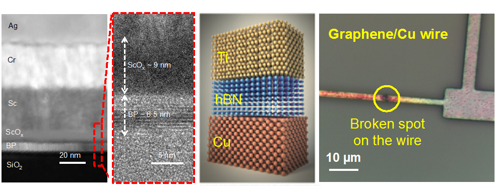
Date and Time
Location
Hosts
Registration
- Date: 15 Aug 2017
- Time: 11:30 AM to 01:30 PM
- All times are (GMT-08:00) US/Pacific
-
 Add Event to Calendar
- Santa Clara, California
- United States
Speakers
Ching-Hua (Fiona) Wang of Stanford University
Topic:
2D Materials Advantages and Challenges Towards Applications
Biography:
Address:Palo Alto, United States