Workshop on Soc Design RTL-GDSII on Cadence Tools
One-week Hands-on Workshop on SoC Design(RTL -GDSII) Using Cadence Tools. This FDP aims at equipping the participants with necessary practical skills and encourages faculty and students to take up careers and research in this area. This FDP will cover SoC Design (RTL –to- GDSII) on Cadence Tools Implement the RTL of a design from its specification Use the Xcelium™ simulator to simulate the design Synthesize the design from RTL to Gates using the Genus™ Synthesis Solution the digital implementation flow with the Innovus™ Implementation
Expert Speakers on Latest Research topics
1. Mohammad Fahim, Principal Engineer , Server SOC division AMD
2. .Mohammed Mateen, Sr Lead Engineer, Qualcomm pvt Ltd
3. Kartik Kailas, Member of Technical Staff, AMD
4. Mohd Ishaq, Senior Emulation engineer, Intel, Hyderabad
5. Mir Riyazath Ali, Senior STA Designer, USA 6.
6. Dr. M. A. Raheem, Assistant Professor, ECED, MJCET
7. Mamidi NagarajuResource persons, Entuple Technologies, Bangalore.
8. Abdul Majid DFT Engineer Nvidia Hyderabad
9. Mr Ghazi Verification Engineer. MiroSemi Hyderabad
Contents:
Day 1: Introduction to Digital ASIC Design – Flow Design Spec and RTL flow Cadence Solutions for Semi Custom IC Design Functional Verification using Incisive tool.
Day 2: Front End Design flow Test automation with TCL gate-level netlist generation Running the Basic Synthesis Flow Counter design, test-bench, Simulation and synthesis. RTL to Synthesis using 90 nm and 45nm Technology generation of report on area, power and quality of results (QoR)
Day 3: Physical Design Flow: (Back-End Stage) Floor Planning, Power-Planning, Placement CTS, Routing, Implementation. Timing Analysis, Power Analysis, Parasitic Extraction Generation of GDSII using Innovus tool.
Day 4: Introduction to SoC Design using Cadence tool Front-end design flow for MSP430 Processor, Introduction to IP Design Flow using 7nm opensource PDK SoC Design ( MSP430 Processor), testbench, elaboration and simulation, RTL Synthesis using Genus Synthesis
Day 5: Back-end design flow for MSP430 Processor Floor Planning Power Planning Placement, CTS Routing Parasitic Extraction Generation of GDSII
Objective of Workshop
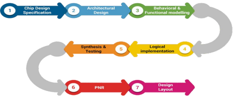
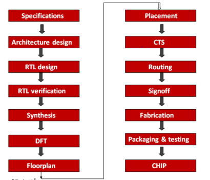
ASIC design flow is a mature and silicon-proven IC design process which includes various steps like design conceptualization, chip optimization, logical/physical implementation, and design validation and verification. Use RTL simulations to verify gate-level designs based on GSSII design-oriented analysis techniques are emphasized throughout the course.
Once the RTL code and testbench are generated, the RTL team works on RTL description – they translate the RTL code into a gate-level netlist using a logical synthesis tool that meets required timing constraints. Thereafter, a synthesized database of the ASIC design is created in the system. When timing constraints are met with the logic synthesis, the design proceeds to the design for testability (DFT) techniques.
After understanding the design specifications, the engineers partition the entire ASIC into multiple functional blocks (hierarchical modules), while keeping in mind ASIC’s best performance, technical feasibility, and resource allocation in terms of area, power, cost and time. Once all the functional blocks are implemented in the architectural document, the engineers need to brainstorm ASIC design partitioning by reusing IPs from previous projects and procuring them from other parties.
As we are moving towards a lower technology node, engineers face complex design challenges with the need for implanting millions of gates in a small area. In order to make this ASIC design routable, placement density range needs to be followed for better QoR. Placement density analysis is an important parameter to get better outcomes with less number of iterations.After routing, ASIC design layout undergoes three steps of physical verification, known as signoff checks. This stage helps to check whether the layout working the way it was designed to. The following checks are followed to avoid any errors just before the tapeout:
1. Layout versus schematic(LVS) is a process of checking that the geometry/layout matches the schematic/netlist.
2. Design rule checks(DRC) is the process of checking that the geometry in the GDS file follows the rules given by the foundry.
3. Logical equivalence checks(LVC) is the process of equivalence check between pre and post design layout.
METHODOLOGY

Outcomes
The workshop was highly rated by participants, particularly for the practical sessions:
Feedback: All participants acknowledged the excellence of the practical sessions, appreciating the individual system access with full licenses.
Written Test Results: Varied results indicated different levels of understanding among participants, reinforcing the need for differentiated follow-up learning.
Conclusions:
The workshop successfully provided a real-time experience of the ASIC design flow, empowering educators and students with the necessary skills to pursue further in this field. The practical approach, combined with expert insights, laid a strong foundation for future endeavors in VLSI design.
Future Recommendations:
Continued support and advanced workshops to cover deeper aspects of VLSI design.
More focused sessions on troubleshooting and optimizing designs to bridge the gap in understanding observed in test results.
Date and Time
Location
Hosts
Registration
- Start time: 20 Jun 2023 08:00 AM
- End time: 24 Jun 2023 05:30 PM
- All times are (UTC+05:30) Chennai
-
 Add Event to Calendar
- MJCET campus
- Hyderabad, Andhra Pradesh
- India 500034
- Building: ECE DEPARTMENT
- Room Number: CADENCE LAB
- Starts 15 June 2023 08:00 AM
- Ends 20 June 2023 08:00 AM
- All times are (UTC+05:30) Chennai
- No Admission Charge
Agenda
The agenda for the one-week Hands-on Workshop on SoC Design (RTL to GDSII) using Cadence Tools, hosted from June 20th to June 24th, 2023 at Muffakham Jah College of Engineering and Technology, is detailed as follows:
Agenda Overview:
Daily Schedule:
9:00-10:00: Lab Practice
10:00-10:05: Short Break
10:05-11:05:Guest Speaker Session
11:05-11:15: Tea Break
1:15-3:00: Intensive Technical Session
3:00-3:45: Lunch Break
3:45-5:00: Lab Session
5:00-6:00: Discussion, Feedback, and Closing Remarks on the last day
Detailed Daily Activities:
Day 1: Introduction to Digital ASIC Design
Morning:
Inaugural Talk: Mohammad Fahim, Principal Engineer, AMD
Session by: Mohammed Mateen, Sr Lead Engineer, Qualcomm
Lab Sessions:
- Introduction to Digital ASIC Design – Flow Design Spec and RTL flow
- Cadence Solutions for Semi Custom IC Design
- Functional Verification using Incisive tool
Day 2: Front End Design Flow
Morning:
Session by: Kartik Kailas, Member of Technical Staff, AMD
Lab Sessions:
- Test automation with TCL
- Gate-level netlist generation
- Running the Basic Synthesis Flow
- Counter design, test-bench, Simulation, and synthesis
- RTL to Synthesis using 90 nm and 45nm Technology generation of report on area, power, and quality of results (QoR)
Day 3: Physical Design Flow (Back-End Stage)
Morning:
Session by:Mohd Ishaq, Senior Emulation Engineer, Intel
Lab Sessions:
- Floor Planning, Power-Planning, Placement, CTS, Routing
- Implementation, Timing Analysis, Power Analysis
- Parasitic Extraction
- Generation of GDSII using Innovus tool
Day 4: Introduction to SoC Design using Cadence Tool
Morning:
Session by: Mir Riyazath Ali, Senior STA Designer, USA (Online)
Lab Sessions:
- Front-end design flow for MSP430 Processor
- Introduction to IP Design Flow using 7nm opensource PDK
- SoC Design (MSP430 Processor), testbench, elaboration, and simulation
- RTL Synthesis using Genus Synthesis
Day 5: Back-end Design Flow for MSP430 Processor
Morning:
Session by: Resource person, Entuple Technologies, Bangalore
Lab Sessions:
- Floor Planning, Power Planning, Placement, CTS, Routing
- Parasitic Extraction
- Generation of GDSII
Valedictory and Feedback Session:
- Conducted on the last day to gather participant feedback and discuss insights and outcomes from the workshop.
Media
| IMAGE1 | 446.88 KiB | |
| IMAGE2 | 165.01 KiB | |
| IMAGE3 | 175.06 KiB |