Nanotech Talk: 2D Materials Advantages and Challenges Towards Applications
2D Materials Advantages and Challenges Towards Applications
Tuesday, August 15, 2017
11:30: Networking, Pizza & Drinks;
Noon -- 1pm: Seminar
Location:
TI Auditorium E1: 2900 Semiconductor Drive. Santa Clara;
speaker:
Ching-Hua (Fiona) Wang, PhD. Student
Electrical Engineering Department, Stanford University
ABSTRACT: Two-dimensional (2D) materials present unique opportunities for next generation ultra-thin electronics. However, practical 2D devices can only be realized after overcoming key challenges: contact resistance, stable doping, and uniform growth.
In this talk I will highlight the recent research our group has implemented to improve contact and doping in BP and MoS2 transistors.
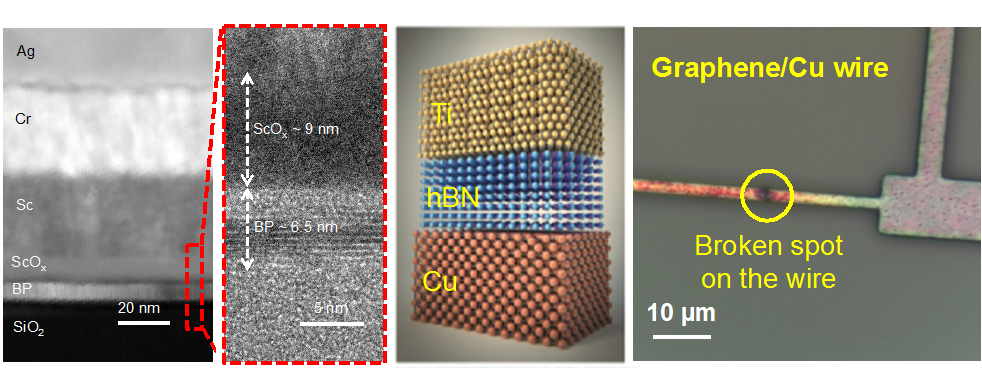
I will then show our work beyond transistor applications using 2D materials, such as graphene-Cu interconnects and hBN-RRAM, that are promising for three-dimensional integrated electronics.
If you have questions or problems with your registration, please contact LincolnBourne@gmail.com
Must Register on eventbrite at:
This event is co-sponsored by IEEE SCV Nanotechnology Council and Young Professionals
Date and Time
Location
Hosts
Registration
-
 Add Event to Calendar
- TI Auditorium E1
- 2900 Semiconductor Drive
- Santa Clara, California
- United States
- Contact Event Host
- Co-sponsored by Nanotechnology Council