PCB Designing Workshop
IAS-PES JOINT CHAPTER, IEEE GCET SB
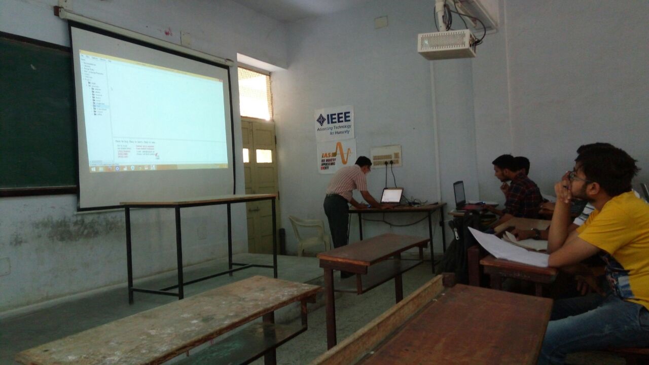
Introduction
IAS-PES Joint Chapter, IEEE GCET SB arranged a workshop on P.C.B Designing for 4th semester EC students. It was conducted in 2 sessions. First session was conducted by Prof. Kavindra Jain, Prof. Neha Upadhayay and Prof. Chetna Shah on 21st February, 2018. Second session was conducted by Dr. Bhaskar Thakkar on 26th February, 2018.
The event was scheduled from 01:30 PM to 03:30 PM.
Session 1
First session was conducted by Prof. Kavindra Jain, Prof. Chetna Shah & Prof. Neha Upadhayay. The session started at 01:30 PM and it focussed on the construction of PCB i.e. how the PCB is being constructed, what are the steps for the construction of PCB. Designing of a PCB is a long process which needs a lot of concentration and knowledge. The software part i.e. the designing/simulating of the PCB can be even done on smart phones through different applications available on the Playstore (e.g.: PCB droid). The following are the information for circuit designing and testing of PCB:-
- Validation to software
- Simulation
- Components testing (if any)
- Creating a GARBAR file
- Converting into .pdf file
- Print on drusy paper
- Ambushing the print on PCB
- Checking the circuit for any cracks
- Filling the same using marker
- Etching the PCB
- Removal of Copper components from PCB except the circuit
- Using sandpaper to remove the rest of the portion after taking it out
- Using solution of baking soda and water to remove the marked circuits
- Cleaning the PCB using water
- Drilling the PCB
- Mounting the set of components
- Soldering the same
- Desoldering the connecting parts.
After completing all the steps you will find that your PCB designing is completed. Basically the session was all about how the PCB board is constructed externally. The session concluded by 03:30 PM.
Session 2
Second session was conducted by Dr. Bhaskar Thakkar. It started at 01:30 PM and the session was all about the software. The session was totally practical, students were given live demonstration of what they were learning. “EAGLE” is the software which was used for the live demonstration. There are many software available for PCB designing. Some key points discussed in the session are:
- .sch = schematic file
- .lbr = library file
- .bdr/.pcb = PCB file
- Footprint = the physical dimension. These are present in the library file.
- Via = Provide bottom layer electrical connection to top layer.
- Polyconeplane = Empty region connected on ground for noise reduction.
- GARBAR file = It has all the information about the tracks in the circuits. It does not have any information about the IC used.
- There are a few sites which can be helpful for getting more information namely sparkfund.com,sunroom.com
The following are the steps to use EAGLE software for construction of PCB:
- Go to ‘Example’
- New folder
- New schematic
- Select library (open)
- Add (search option is available)
- Grid option (show lines)
- Prepare the circuit
- Tools (autorouter)
- Select layer and then “/” or N/A or Auto
- Route (to change the width of the ned)
- Change (will provide the option to change various parameters)
- Generate the GARBAR file
After completing all the above steps the internal designing of the PCB is completed. This session successfully concluded at 03:30 PM.
Date and Time
Location
Hosts
Registration
-
 Add Event to Calendar
- Anand, Gujarat
- India 388120
- Starts 17 February 2018 03:30 AM UTC
- Ends 19 February 2018 12:00 PM UTC
- No Admission Charge
Speakers
Prof. Kavindra Jain of G H Patel College of Engineering & Technology
Construction of PCB
Prof. Kavindra Rajeevkumar Jain completed in 2006 his Bachelor of Engineering with specialization in Electronics & Instrumentation, with 76.49%, twice merit list holder in Punjab Technical University & secured 2nd position in college as well as third rank holder of University,from Guru Teg Bahadar Khalsa Institute of Engg & Technology,Chhapianwali Malout. He completed his Master of Engineering with specialization in Electronics & Communication in August 2009, with 7.22(CPI) , from G.H.Patel College of Engg. & Technology,V.V.Nagar, Anand, Gujarat.Presently he is pursuing his Ph.D from R K University,Rajkot since May 2013. He has more than 10 years of teaching and research experience. His area of interest includes Image processing, computer vision,machine vision technology and medical image analysis. He has guided 15+ M.E. students in their dissertation as well as more than 12 UG level final year projects groups. He has published more then 45 Research papers in various International and National Journals and conferences. He has organized more than 35 workshops for undergraduate students in various domains of Integrated Circuit and Applications,Basic Electronics, Power Electronics,Labview and Matlab as well. He has delivered expert talk on image processing and organized Latex based workshop in other institutes as well. He has been working as TPC member and Reviewer of several international IEEE conferences. He has organized twice STTP of one week duration on image processing with Technical support of IEEE SPS chapter in college.
Address:Anand, Gujarat, India, 388120
Dr. Bhaskar Thakkar of G H Patel College of Engineering & Technology
PCB Design
Dr. Bhaskar Thakkar obtained Ph.D. from Indian Institute of Technology Delhi in March 2013. He graduated from Birla Vishvakarma Mahavidyalaya in year 1997 and completed his Masters of Engineering in Microprocessor Systems & Applications from M S University Baroda in year 2000. Dr. Bhaskar has authored 2 books and published around 30 research articles in various International and National Journals and Conferences. His main areas of interest are Biomedical Signal Processing & Analysis, Embedded System Design, Wireless Sensor Network Designand Instrumentation.
Dr. Bhaskar Thakkar is actively involved in R&D projects and handled several Consultancy projects in past. He has got involved in a collaborative Research project between Loughborough University, UK and IIT Delhi, India under UKIERI (UK- INDIA Education and Research Initiative) program with title "Communication Technology for Monitoring Heart Disease & Diabetes" during year 2008 - 2011. He has worked as Co-Principal Investigator in an R & D Project from Department of Information and Communication Technology, with title "Wireless Body Area Network for Health Monitoring" where IIT Delhi and GCET were associated. He has visited countries like UK, China and Malaysia for the research activity. Dr. Bhaskar is a Principle Investigator for a Minor Research Project (MRP) sanctioned by GUJCOST (Gujarat Council on Science and Technology) with title "Wrist Pulse Monitoring and Recording System for assisting in Ayurveda based Health Diagnosis" with amount Rs. 5.0 Lakh. January 2014 - December 2016. He is serving GCET for last 18 years.
Address:Anand, Gujarat, India, 388120