INTERNATIONAL INVITATIONAL SYMPOSIUM ON NANOMATERIALS AND NANOCOMPOSITES PROCESSING, SYNTHESIS & APPLICATIONS
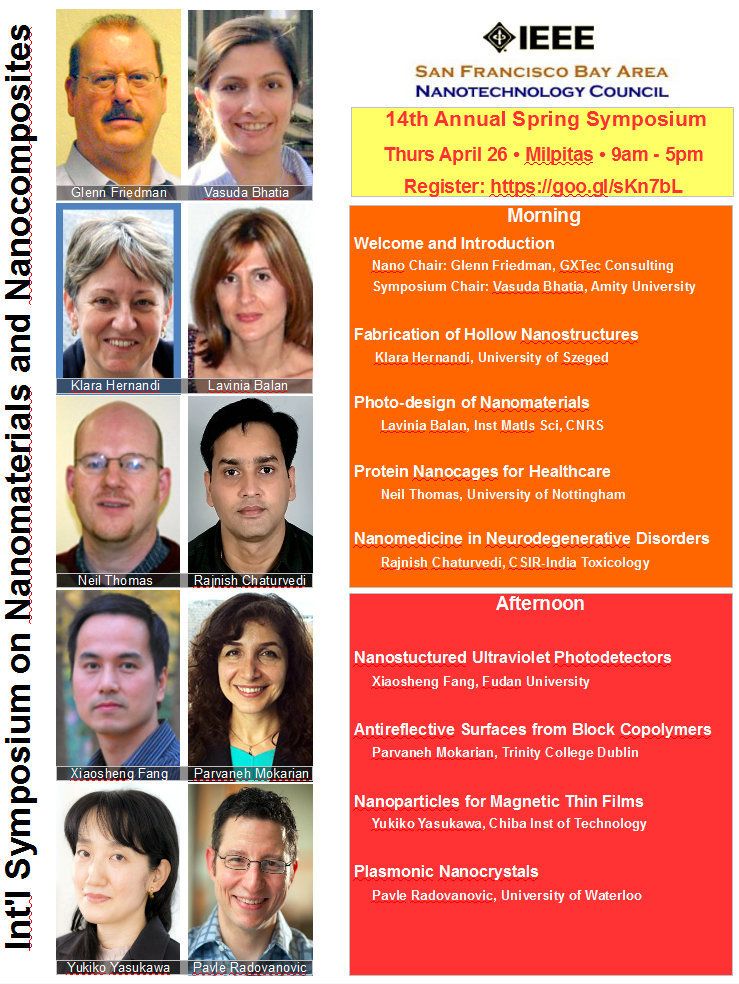
SFBA Nanotechnology Council's 14th Annual Spring Symposium
Bringing together leading academic, government and industry experts to discuss innovative opportunities and technical challenges associated with nanotechnology.
Presentations and Networking opportunities
Register at Eventbrite:htttps://goo.gl/sKn7bL

Date and Time
Location
Hosts
Registration
- Date: 26 Apr 2018
- Time: 04:00 PM UTC to 01:00 AM UTC
-
 Add Event to Calendar
- SEMI Global Headquarters
- 673 South Milpitas Boulevard
- Milpitas, California
- United States CA 95035
- Starts 01 March 2018 07:00 PM UTC
- Ends 26 April 2018 01:00 AM UTC
- No Admission Charge
Speakers
Prof. Klara Hernadi of Department of Applied and Environmental Chemistry, University of Szeged, Hungary
Fabrication of Hollow Nanostructures
Hollow materials generally show better performance than their solid counterparts thus they are excellent candidates for various applications in the fields of energy, environment, health, or sensing. However, their fabrication can be challenging therefore scientific community attends to their selective synthesis. In my talk I am going to give a brief summary about the syntheses of both carbon nanotube forests and spherical semiconductors.
Potential applications of carbon nanotubes (CNTs) can be significantly widen, in case CNTs form a forest-like, vertically aligned structure (VACNT). The aim of our experiments was to develop a cheap and easy method for growing carbon nanotubes forests on various substrates (either conductive or non-conductive) with the CCVD (Catalytic Chemical Vapor Deposition) method. However, this growth technique is rather sensitive to synthesis parameters both during catalyst layer formation (substrate; composition; thickness; porosity; etc.) and during CCVD (gas feed – carbon source, carrier, hydrogen, water vapor; reaction temperature; reaction time; etc.). In order to tune the height of vertically aligned carbon nanotube forest several parameters were varied during both catalyst layer fabrication (e.g. ink concentration, ink composition, dipping speed) and CCVD synthesis (e.g. gas feeds, reaction time). It was established that no considerable alignment occurs when CNTs are shorter than 10 μm. Authors are convinced that simple and cheap methods for CNT forest growth can open up novel applications in nanotechnology devices.
Semiconductor hollow structures are of growing interest in the field of photocatalysis. These objects are interesting not just because of their low apparent density but also their unique optical properties. For the synthesis of either carbon-metal oxide composites or hollow semiconductor structures, nanometer sized carbon spheres (CS) were prepared by mild hydrothermal treatment of ordinary table sugar (sucrose). The size of these spheres can be controlled by the parameters of the hydrothermal treatment (e.g. time and pH). CSs were successfully coated with TiO2 and ZnO via either sol-gel method or atomic layer deposition. Subsequently, burning out the carbon core templates resulted in hollow metal oxide nanospheres. The unique hollow sphere morphology proved to enhance the photocatalytic activity (six times) as well as TOC removal efficiency (twelve times) compared to the sample which was prepared by the same method without the CSs.
Prof. Xiaosheng Fang of Department of Materials Science, Fudan University, Shanghai, Chaina
ZnO Micro/Nanostuctures Based Ultraviolet Photodetectors
ZnO micro/nanostructures has been paid significant attentions in ultraviolet photodetectors due to their wide bandgap (3.37 eV), abundant morphologies and ease preparation methods. Typically, post prepared ZnO micro/nanostructures show intrinsic n-type property and p-type ZnO is rather difficult to be realized. In this talk, we present various researches of composite structural ultraviolet photodetectors based on composite heterostructures between ZnO and different p-/n- type materials (such as SnO2@ZnO core-shell, ZnO@Ga2O3 core-shell, ZnO/BiOCl heterostructures et al.). The two different semiconductors were artfully chosen to meet the requirement of forming type-II heterojunction (i.e., staggered gap). Therefore, in all of these devices, self-powered characteristic was shown because of the photogenerated electron-hole pairs can be collected by the built-in electric field. Our device design method would provide a new approach to realize the high performance energy saving photodetectors.