Low Power Deep Submicron Designs
The talk provides an overview of techniques utilized for achieving low power implementation for deep sub-micron digital design. Major contributors for power dissipation in digital CMOS designs will be described. The power analysis and the power variation with respect to technology parameters and the design style will be explained. The power management techniques such as shutting down portions of design will be described. The formal power management specification such as UPF / CPF will be covered. Other advanced techniques such as voltage scaling (static or dynamic) will be described.
Date and Time
Location
Hosts
Registration
-
 Add Event to Calendar
- 161 Warren St
- Newark, New Jersey
- United States 07102
- Building: ECE Building
- Room Number: 202
- Click here for Map
- Contact Event Host
- Durga Misra (973) 596-5739 (dmisra “AT†njit.edu) or Dr. Edip Niver (973) 596-3542 (NJIT)
- Co-sponsored by ECE Dept, NJIT
Speakers
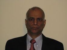
 Rakesh Chadha of eSilicon Corporation
Low Power Deep Submicron Designs
The talk provides an overview of techniques utilized for achieving low power implementation for deep submicron digital design. Major contributors for power dissipation in digital CMOS designs will be described. The power analysis and the power variation with respect to technology parameters and the design style will be explained. The power management techniques such as shutting down portions of design will be described. The formal power management specification such as UPF / CPF will be covered. Other advanced techniques such as voltage scaling (static or dynamic) will be described.
Biography: Dr. Rakesh Chadha is an ASIC design specialist with over 25 years of experience in timing and signal integrity at Bell Laboratories, Cadence and eSilicon. He was responsible for the timing and signal integrity for the Sematech project on Chip Parasitic Extraction and Signal Integrity Verification. He has been responsible for complex SOC design methodology for several generations of process technologies. He holds a PH.D. degree in Electrical Engineering from the Indian Institute of Technology, Kanpur.
Email:
Address:890 Mountain Avenue, Suite 215, , New Providence, New Jersey, United States, 07974
Rakesh Chadha of eSilicon Corporation
Low Power Deep Submicron Designs
Biography:
Email:
Address:New Providence, New Jersey, United States
Agenda
Talk at 7:00 pm
ECE 202, 161 Warren Street, NJIT, Newark, NJ
You don't have to be a member of IEEE to attend this meeting
