Switzerland & Italy Joint IEEE Day online celebration

Dear IEEE Members,
We have the pleasure to Invite you to join us in celebrating IEEE Day.
In this occasion Italy and Switzerland Section together with organisation unit prepared for you a program bridging the past and the future.
The program is as follow :
18:00-18:10 Opening Session
The chair of Switzerland and Italy Section will introduce the session
18:10-19:10 : The microchip revolution
Representatives of the Life Members and History activities of Switzerland and Italy brought up a session around the theme of The microchip revolution.
- It is our great pleasure to convey a meeting with the participation of
1. Luc-Olivier Bauer and Marshall Wilder authors of the book "The Microchip Revolution: A brief history".
The Book is available online and we encourage you to read.
The book was dedicated to the memory of Dr.Jean Amédée Hoerni (1924-1997), a Swiss Geneva born scientist expatriated first to
Cambridge, then Caltech, hired by Bill Shockley at his Mountain View Labs, who become the only non American partner of the
“traitorous eight engineers“ founders in 1957 of Fairchild Semiconductors in Palo Alto.
He filed the fundamental patent on the Planar Process there in 1959.
And subsequently together with Bob Noyce the patent on silicon integrated circuits.
Also know as as silicon chips, e.g. microchips. The rest is history!
2. Bruno Murari of ST-Microelectronics
Will present a contribuiton on BCD technology entitled Multiple Silicon Technologies on a Chip.
From research to a successful industry standard
The session will be interactive and moderated by Hugo Wyss From the Swiss Life Members Section.
Togerther With Mathier Coustans & Taekwang Jang From the Solid State chapter Switzerland
19:15-20:15 : IEEE STUDENT BRANCH & YOUNG PROFESSIONAL PITCH : 5 MINUTES FOR MY RESEARCH
Bridging the past and the future.
10 Student and Young Professionalare going to pitch their research topic.
Your vote are expected to elect the best presenter
20.15-20.20 Closing Session
*Privacy statement : We do our best for privacy, nevertheless online meeting and 999 participant may take on their own snapshot, find their own recording tools, which we cannot control. Thus we ask you to adapt an adequate behavior for information you wont like to share. such as making sure any content share is fine to be public, and approved. Limit distractions and maintain privacy in your current surroundings by using a virtual background. You can blur your background, change your background, or add a background image during your meeting.
Date and Time
Location
Hosts
Registration
-
 Add Event to Calendar
Loading virtual attendance info...
- Starts 15 September 2020 08:00 PM UTC
- Ends 06 October 2020 03:50 PM UTC
- No Admission Charge
Speakers
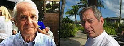 Luc-Olivier Bauer
The Microchip Revolution: A brief history
Numerous books have been written about the key founders of the semiconductor industry, about the early companies, the reasons for their success and failures, on the star products, and the men behind them.In conversations with the Computer History Museum (CHM) of Mountain View, California, the two authors, veterans of semiconductor manufacturing organizations, found that the history of semiconductor process development has been treated as an ancillary issue in top down discussions of what drove the extraordinary growth of this industry. We tell the story from a bottom-up point of view of wafer fab operation managers, which we were for many years. We narrate the extraordinary contributions from all team members of these wafer fab organizations: hourly operators, supervisors, maintenance technicians, as well as the creative scientists and engineers that created and managed the companies we profile. We concentrate on the dramatic improvements in manufacturing productivity in the main MOS technologies, which eventually all merged into very similar CMOS processes. We concentrate on the time period from 1957 (Fairchild founding) to the end of the last century, when much of the technology development migrated to foundry operations overseas. We tried to exercise great care to be fair in assessing the contributions of the various companies to the overall progress of the industry.In this spirit, we also recognize the huge contributions made by the semiconductor equipment companies, and their key engineers to the success of process development and production organizations.While basing the story of process developments on historical facts, with the help of the large document and library resources available, including those of the CHM, we also tell the extraordinary human experience of working with the early wafer fab teams, with the process architecture breakthroughs pioneers, and all other wafer fab workers. To this end we also interviewed many key contributors to these process and equipment breakthroughs that made the rapid advancements in the semiconductor technologies possible.
Biography:
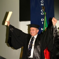 Bruno Murari
Multiple Silicon Technologies on a Chip : from research to a successful industry standard
In the sixties the technical community started to integrate successfully on silicon many transistors to miniaturize electronics equipment including increasingly complex electronic functions in limited space with minimum weight.
In any electronic system several key functions are present as in any human being.
Brain is realized complex integrated circuits performing complex operations and storing the information in different memory systems. Muscles are need to (re) act once the information has been properly processed and the making decision has been taken.
Different evolution branches generated all along the years: the digital one and the more heterogeneous Power and Analog ones. In the digital area the progress followed until today the well-known Moore law: ‘…The complexity for minimum component costs has increased at a rate of roughly a factor of two per year…. Over the longer term, the rate of increase is a bit more uncertain, although there is no reason to believe it will not remain nearly constant for at least 10 years….’ (‘Cramming more components onto integrated circuits’, G. Moore, 1965). A new CMOS technology generation has been made regularly available (every 2-2.5 years) to address higher performance, low power computing and increased density requirements sustained today by new emerged applications (smart phone, data centers, communication infrastructure). At the same time Power Integrated Circuits were originally realized using pure bipolar technologies driven by the audio amplifier market segment evolution. Bipolar transistors were widely used both for the realization of power stages and for the integration of the required analog functions thanks to their outstanding linearity behavior.
Bipolar transistors limitation in handling efficiently large power delivery together with the poor logic scaling performance put major challenges in managing the efficient integration of the different functions onto a single silicon die.
In 1984, STMicroelectronics had the insight to mix process technologies combining Bipolar, CMOS and power DMOS transistors (first BCD technology platform) to build fully integrated complex system on a single chip. In 1985 SGS (at that time it was the name of ST) in its research laboratories, developed the first integrated circuit: a switching bridge control system for DC and stepping motors (60V, 5A) working at 300KHz with the best efficiency.
This was the first SGS commercial product realized with BCD technology on the market.
In the following 35 years, Multipower BCD has become widely adopted by Automotive, Industrial and Consumer industries becoming one of several standard platforms in semiconductor industry.
Functions integration has followed multiple paths. On one side thanks to the availability of mature CMOS technology, increasing amount of digital functions and memory has been integrated with analog and power devices. Major challenges have been faced on one side in the technology development to merge in a single platform increasingly complex CMOS devices with high performance Power transistor. At the same time complex IC design has required major efforts in the process architecture and characterization to enable the successful integration of complex logic cores and memory with large current Power stages
Today a complete motor control system can be embedded on a single die including a microcontroller with the Power stages delivering the current need to act motor motion
On the other side the integrated functions. At the same time, the number of integrated functions has been continuously increased thanks to the increased knowledge and engineering efforts. Today in a modern Hard Disk drive system in a Power IC the disk motor driving stages are integrated in the same die with several Switching Power regulators supplying the different Complex ASIC present in the system.
The success story is still going on and advanced technology nodes down to 40nm with embedded non-volatile memory solutions are today announced enabling added intelligence for monitoring and control. Voltage capability is provided up to 2000V and even on-die Galvanic isolation from different grounds up to 10kV can be realized. Considering this road map vision, the challenge is an intellectual stimulus for young engineers to utilize renovate technology for next multipower generation
Biography:
Bruno Murari is a Scientific Advisor to ST and some R&D centers and corporations in Italy, France and Switzerland, after his retirement as the Director of the ST Castelletto R&D laboratories in Milan, Italy.
Murari started his career at Edison Volta and ENI and joined SGS -- now STMicroelectronics -- in 1961. In 1972 he became head of linear IC design and development and in 1981 was appointed to lead the Castelletto site – an R&D center and fab for smart-power ICs, MEMS (Micro-Electro-Mechanical Systems), and photonics. Murari has significantly contributed to ST's leadership position in high-power IC technology, through designing and supervising the design of more than 2000 ICs, producing over 80 patents.
Murari has led the development, technology transfer, and ramp-up of micromachining technology for MEMS, a segment in which ST has become a pioneer and world leader. In 2011 he received the SAPIO award for Industry from the President of Italy’s Republic.
Born in Treviso in 1936, Murari earned a degree in Electrical Technology from Pacinotti Technical Institute and a postgraduate degree in electronics from Beltrami Institute, Milan. In 2002 he received an Honorary Degree in Electronic Engineering from Politecnico of Milan for fundamental innovations in semiconductor technologies and IC design.