Autodesk PCB Design Tutorial
#Printed
#Circuit
#Board
#(PCB);
#Eagle;
#Fusion
#360;
#Autodesk;
#Introduction;
#Beginner


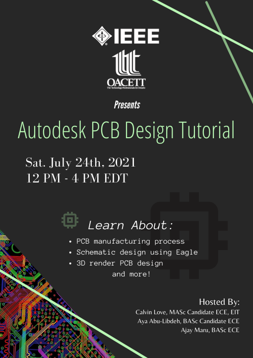
The tutorial session is intended to walk students through the PCB design process using the Autodesk Suite (Eagle and Fusion 360). This lecture is broken up into 3 sections in order to achieve the following learning outcomes:
1. Advantages and disadvantages of PCB design vs conventional circuit prototyping methods and the PCB fabrication process.
2. Develop a library of parts including the schematic symbol, 2D PCB footprint and 3D package design.
3. Convert a circuit schematic into a PCB design to be sent to the manufacturer for fabrication.
4. 3D render PCB Design.
Date and Time
Location
Hosts
Registration
-
 Add Event to Calendar
Loading virtual attendance info...
- Windsor, Ontario
- Canada
- Contact Event Hosts
-
Calvin Love
- Co-sponsored by OACETT
- Starts 11 July 2021 04:00 AM UTC
- Ends 24 July 2021 04:00 PM UTC
- 1 in-person space left!
- No Admission Charge
Speakers
 Calvin Love of OACETT
Email:
Address:Ontario, Canada
 Aya Abu-Libdeh
Email:
Address:Ontario, Canada