Semiconductor workforce development through immersive simulations on nanoHUB.org
Gerhard Klimeck , Purdue
Fellow IEEE, APS, IOP, AAAS, and Humboldt Foundation
Abstract:
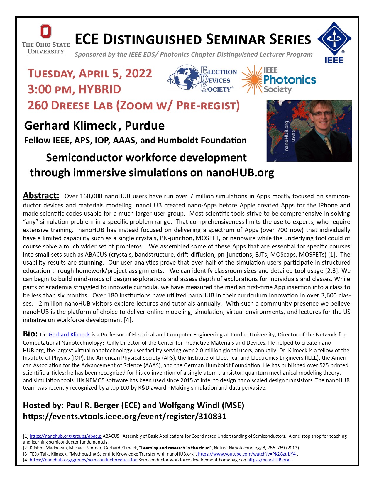
Over 160,000 nanoHUB users have run over 7 million simulations in Apps mostly focused on semiconductor devices and materials modeling. nanoHUB created nano-Apps before Apple created Apps for the iPhone and made scientific codes usable for a much larger user group. Most scientific tools strive to be comprehensive in solving “any” simulation problem in a specific problem range. That comprehensiveness limits the use to experts, who require extensive training. nanoHUB has instead focused on delivering a spectrum of Apps (over 700 now) that individually have a limited capability such as a single crystals, PN-junction, MOSFET, or nanowire while the underlying tool could of course solve a much wider set of problems. We assembled some of these Apps that are essential for specific courses into small sets such as ABACUS (crystals, bandstructure, drift-diffusion, pn-junctions, BJTs, MOScaps, MOSFETs) [1]. The usability results are stunning. Our user analytics prove that over half of the simulation users participate in structured education through homework/project assignments. We can identify classroom sizes and detailed tool usage [2,3]. We can begin to build mind-maps of design explorations and assess depth of explorations for individuals and classes. While parts of academia struggled to innovate curricula, we have measured the median first-time App insertion into a class to be less than six months. Over 180 institutions have utilized nanoHUB in their curriculum innovation in over 3,600 classes. 2 million nanoHUB visitors explore lectures and tutorials annually. With such a community presence we believe nanoHUB is the platform of choice to deliver online modeling, simulation, virtual environments, and lectures for the US initiative on workforce development [4].
[1] https://nanohub.org/groups/abacus ABACUS - Assembly of Basic Applications for Coordinated Understanding of Semiconductors. A one-stop-shop for teaching and learning semiconductor fundamentals.
[2] Krishna Madhavan, Michael Zentner, Gerhard Klimeck, "Learning and research in the cloud", Nature Nanotechnology 8, 786–789 (2013)
[3] TEDx Talk, Klimeck, “Mythbusting Scientific Knowledge Transfer with nanoHUB.org”, https://www.youtube.com/watch?v=PK2GztIfJY4 .
[4] https://nanohub.org/groups/semiconductoreducation Semiconductor workforce development homepage on https://nanoHUB.org .
Date and Time
Location
Hosts
Registration
-
 Add Event to Calendar
Loading virtual attendance info...
- 2015 Neil Avenue
- Columbus, Ohio
- United States 43210
- Building: Dreese
- Room Number: 260
- Click here for Map
- Starts 03 April 2022 04:34 PM UTC
- Ends 05 April 2022 07:15 PM UTC
- No Admission Charge
Hosted by: Paul R. Berger (ECE) and Wolfgang Windl (MSE)