Photocurrent and Noise Analysis as Alternative Approaches to Understanding OFET Behavior
The characterization of organic field effect transistors is complicated by the influence of the contacts on channel behavior and the trap limited conduction mechanism which governs device performance.
In this presentation, several strategies for probing OFETs will be discussed. In particular, the use of spectrally resolved photocurrent spectroscopy will be demonstrated as a strategy for the analysis of trap states in the device, spatially resolved photocurrent will be presented as an approach for measuring internal device potential, and noise spectroscopy will be presented as an approach to evaluating the effect of trap states on channel conduction. These probes provide additional pathways for analyzing OFET device and material behavior with different complicating parasitics than incumbent characterization approaches.
Date and Time
Location
Hosts
Registration
-
 Add Event to Calendar
- 161 Warren Street
- Newark, New Jersey
- United States 07102
- Building: ECE Building, Room 202, NJIT
- Click here for Map
- Contact Event Host
- Dr. Durga Misra (973) 596-5739 (dmisra “AT†njit.edu) or Dr. Edip Niver (973) 596-3542 (NJIT)
- Co-sponsored by NJIT
Speakers
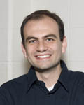
 Ioannis (John) Kymissis of Columbia University SEAS
Photocurrent and Noise Analysis as Alternative Approaches to Understanding OFET Behavior
The characterization of organic field effect transistors is complicated by the influence of the contacts on channel behavior and the trap limited conduction mechanism which governs device performance. In this presentation, several strategies for probing OFETs will be discussed. In particular, the use of spectrally resolved photocurrent spectroscopy will be demonstrated as a strategy for the analysis of trap states in the device, spatially resolved photocurrent will be presented as an approach for measuring internal device potential, and noise spectroscopy will be presented as an approach to evaluating the effect of trap states on channel conduction. These probes provide additional pathways for analyzing OFET device and material behavior with different complicating parasitics than incumbent characterization approaches.
Biography:
Ioannis (John) graduated with his SB, M.Eng., and Ph.D. degrees from
MIT. His M.Eng. thesis was done as a co-op at the IBM TJ Watson
Research Lab on organic thin film transistors, and his Ph.D. was in
the Microsystems Technology Lab at MIT working on field emission
displays. After graduation he spent three years as a post-doc in MIT's
Laboratory for Organic Optics and Electronics working on a variety of
organic electronic devices and as a consulting engineer for QDVision,
which is developing and commercializing a novel light emitting
architecture based on quantum dots. In 2006, John joined the
Electrical Engineering department at Columbia University and leads the
Columbia Laboratory for Unconventional Electronics (CLUE) which
focuses on the development and applications of thin film electronic
systems.
Email:
Address:Columbia University SEAS, Room 1300/MC 4712, 500 W120th Street, New York, New York, United States, 10027
Ioannis (John) Kymissis of Columbia University SEAS
Photocurrent and Noise Analysis as Alternative Approaches to Understanding OFET Behavior
Biography:
Email:
Address:New York, New York, United States
Agenda
4:45 PM: Pizza & Soda
5:00 PM: Talk

