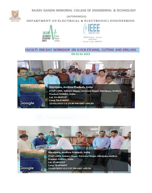
FACULTY ONE-DAY WORKSHOP ON PCB ETCHING, CUTTING AND DRILLING
IEEE-IAS SPONSORED FACULTY ONE-DAY WORKSHOP ON
PCB ETCHING, CUTTING AND DRILLING
PCB drilling (which is also known as printed circuit board drilling), is the process of creating holes, slots and other cavities in an electronic circuit board. During the PCB drilling process, a number of different hole types are drilled.
PCB etching is the process of removing unwanted copper from a printed circuit board. Once all of the excess copper has been removed from the PCB, only the required circuit remains. Before the etching process begins, a layout for the board is generated.
Date and Time
Location
Hosts
Registration
- Date: 22 Feb 2023
- Time: 04:30 AM UTC to 10:30 AM UTC
-
 Add Event to Calendar
- NH-40, Nerawada Post.,Nandyal-518501
- Rajeev Gandhi memorial College of Engineering & Technology
- NANDYAL-518501, Andhra Pradesh
- India 518501
- Building: Dept. of EEE
- Room Number: Power Electronics Lab PG 3130
- Starts 20 February 2023 04:30 AM UTC
- Ends 21 February 2023 11:30 AM UTC
- No Admission Charge
Speakers
 Mr.Krishna of Acte Technologies
PCB etching
PCB etching is one of the most important elements of the PCB manufacturing process. It involves removing copper from the surface of the PCB in order to reveal the desired circuit pattern.
During the PCB etching process, all copper is removed except for the circuitry that is protected by tin plating. Following this, the tin is then stripped and the copper is cleaned.
Although it sounds straightforward, the PCB etching process is quite complex and precision is vital. Plus, various methods of PCB etching can be employed, and each of these has its own benefits and drawbacks.
To help you understand the PCB etching process in greater detail, we’ve put together this guide. As well as covering what PCB etching is and where it sits within the PCB manufacturing process, we’ve also outlined how we etch PCBs and how we can help meet your needs.
Email:
Address:Abbayyas 2, Lane Adj. Karachi Bakery, Madhapur Hyderabad - 500081 Telangana, India Landmark - Near Indian Bank, Vittal Rao Nagar, , Hyderabad, India, 500081
ORGANISED BY DEPT.OF EEE,R G M COLLEGE OF ENGINEERING & TECHNOLOGY ON 22-02-2023