Short Term Skill Development Program (SDP) On Analog Circuit Design & Layout using Cadence EDA Software
Analog Circuit Design & Layout Using Cadence EDA Software
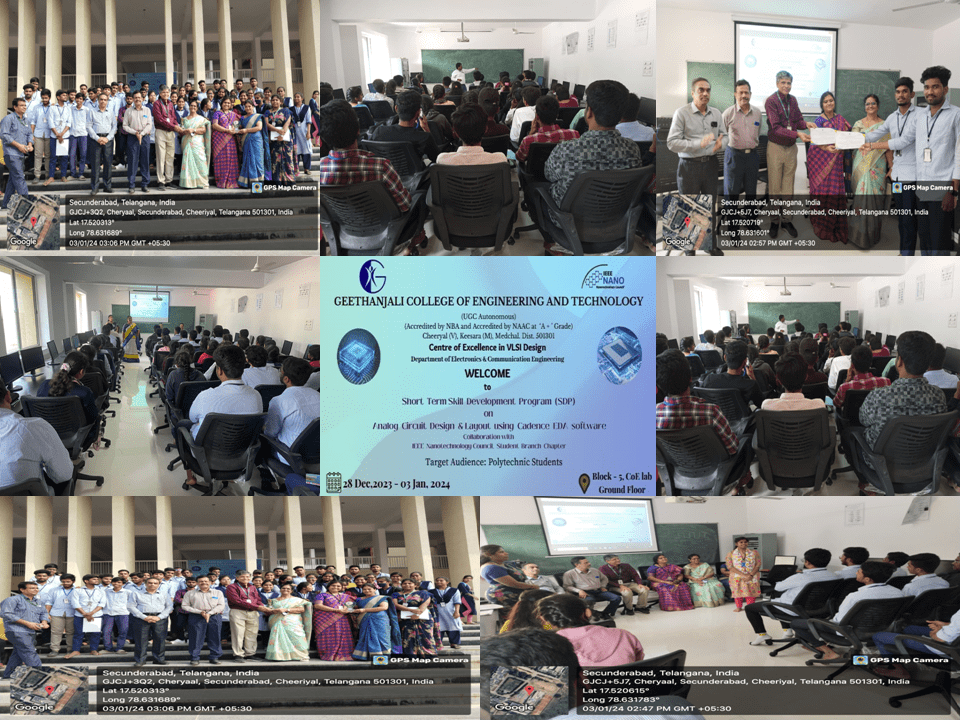
The main objective of this Student development program is to provide a platform for
polytechnic students to enhance their skills in the field of VLSI Design and learn to design
VLSI projects using Cadence tools
The session also aims to enlighten the participants who wish to enhance their skills in the
area of VLSI technology, and this would be a motivation for them towards job opportunities
in this area as well as to pursue the research.
Develop ability to
Understand the basics of VLSI Design
Understand basics of Cadence Tools.
Design projects using Cadence Tool
Understand how this field helpful for employment
Date and Time
Location
Hosts
Registration
-
 Add Event to Calendar
- Geethanjali college of Engineering and Technology
- Cheeryal,Keesara
- Medchal, Andhra Pradesh
- India 501301
- Building: 5
- Room Number: CoE lab
- Starts 25 December 2023 04:00 AM UTC
- Ends 27 December 2023 10:00 AM UTC
- No Admission Charge
Speakers
Dr.G Sreelakshmi
Introduction to VLSI
The objective of the SDP is to provide hands-on experience on the state-of-
the-art Cadence EDA tools for VLSI Design. The participants will have
exposure to Circuit Design, Simulation, Layout, Physical Verification (DRC,
LVS), and Extraction.
SDP Topics
Introduction to VLSI Design Flow
CMOS, Complex Logic Gates using Cadence Virtuoso.
Common Source Amplifier Layout, DRC / LVS & Practice Sessions
Implementation of Micro- Projects.
Prof. O.V.P.R Siva Kumar
CMOS Inverter Characteristics using Cadence Virtuoso, Layout Design, and DRC/LVS by Assura.
Agenda
1. 28/12/2023 (FN)
9:00 AM to 12:30PM
Introduction to Analog Design Flow,
Basics of MOS Technologies,
Introduction to Cadence Virtuoso
Tools
2. 28/12/2023 (AN)
1:00 PM to 3:30PM
CMOS Inverter Design
Schematic, Symbol and Simulation
3. 29/12/2023 (FN)
9:00 AM to 12:30PM
CMOS Inverter Layout,
DRC/LVS, Extraction of RC
Parameters
4. 29/12/2023 (AN)
1:00 PM to 3:30PM
Graphic Design System (GDSII)
Flow
Design of Complex Logic gates
5. 30/12/2023 (FN)
9:00 AM to 12:30PM
Design of Complex Logic gates
6. 30/12/2023 (AN)
1:00 PM to 3:30PM
Design of Common Source Amplifier
7. 02/01/2024 Implementation of Micro project
8. 03/01/2024 (FN)
9:00 AM to 12:30PM
Projects Presentation
9. 03/01/2024(AN)
1:00 PM to 3:30PM
Best Project Announcement,
Suggestions by Professors, Certificate
distribution &Feedback collection
https://docs.google.com/document/d/1ZJjD8Pp3ZGvQetJkJKz9bU9Ej2TzkALq/edit?usp=sharing&ouid=107981588534814759374&rtpof=true&sd=true