Quantum Dots: History, Challenges, and Perspectives
Celebrating 40 years of groundbreaking research in the field of quantum dots, from the early pioneering studies to the latest developments in quantum technologies.
Overview
In 1985, the landmark paper titled “Growth by Molecular Beam Epitaxy and Characterization of InAs/GaAs Strained-Layer Superlattice” was published, marking the start of a new era in the study of quantum dots. Over the past four decades, this field has grown into a vibrant interdisciplinary area of research, intertwining materials physics, advanced characterization techniques, nanotechnology, optics, and quantum technologies. Quantum dots have become key components in a wide range of applications, from optoelectronics and photonics to quantum computing and communication systems.
Agenda
14:00 - 15:00 - Professor Claude Weisbuch (IP Paris & UC Santa Barbara, USA)
Keynote Lecture: The long saga of quantum size effects in semiconductors and of their applications: From quantum dots to quantum wells, … back to quantum dots
15:00 - 15:30 - Break
15:30 - 16:30 - Dr. Jean-Michel Gérard (CEA LETI)
Keynote Lecture: Self-assembled quantum dots, from a discovery by chance to key applications in quantum photonics
16:40 - 17:10 - Round Table Discussion
Challenges and Future Perspectives in Quantum Dot Research
17:15 - 18:15 - Cocktail Reception, Networking and Discussion
Date and Time
Location
Hosts
Registration
-
 Add Event to Calendar
Loading virtual attendance info...
- TELECOM PARIS
- 19 place Marguerite Perey
- Palaiseau, Ile-de-France
- France 91120
- Room Number: Amphi 2
- Contact Event Host
-
- Co-sponsored by Société Française d'Optique
Speakers
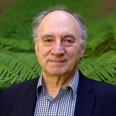
Professor Claude Weisbuch
The long saga of quantum size effects in semiconductors and of their applications: From quantum dots to quantum wells, … back to quantum dots
3D nanostructures existed well before the 2D quantized systems, in metals or semiconductors: many ways exist to fabricate, controllably or not, 3D nanostructures, the most well-known being colloids, with forerunners being precipitates in doped glasses.
Quantum size effects in 2D were identified thanks to the progress in thin film growth, and 2D phenomena at semiconductor interfaces came naturally following the surface effects which lead to the point contact transistor in 1947.
A major breakthrough came in 1974 with the size quantization in quantum wells (QWs) grown by MBE. QWs are now the dominant active layer of semiconductor lasers. Their success comes from the matching of the numbers of inverted states at transparency and of states producing gain to reach threshold, a circumstance not reproduced when going to lower dimensionalities.
However, many efforts were devoted to the fabrication of semiconductor quantum dots, either by top down (etching) or bottom up (self-organized growth) methods.
The impact of low dimensions leads to changes in the light-matter interaction: 2D QWs interacting with 2D photon states in microcavities led to the strongly-coupled cavity polaritons, a new state of matter exhibiting unique properties such as Bose Einstein condensation or superfluidity. 0D excitations of QDs interacting resonantly with 0D photons in 3D cavities lead to the Purcell factor enhancement of spontaneous emission, a welcome factor in high-rate single photon emitters. Lastly, QDs within matrices with high defect density retain high efficiency thanks to their localization effect leading to the avoidance of non-radiative centers.
Biography:
Claude Weisbuch is a semiconductor physicist. He held positions in academia, industry, government.
He is now an emeritus “Directeur de Recherche” at the Centre National de la Recherche Scientifique (CNRS) at Ecole Polytechnique, France and a Distinguished Professor in the materials department of University of California at Santa Barbara. He has been at Bell Laboratories (1979-1981), at Saint Gobain and Thomson-CSF (now Thales). He was “directeur scientifique” (chief scientist) of Délégation Générale pour l’Armement (procurement), ministry of defense, France, 1992 - 1998.
He founded in 2002 a high-tech company, Genewave, Paris, devoted to fluorescence based molecular diagnostics systems, which merged in 2014 with Mobidiag and was acquired by Hologic in 2021.
He has authored or co-authored more than 260 papers and 35 patents. Since 1993, he worked on light extraction in LEDs through microcavities and photonic crystals, and since 2013 on fundamental processes in nitride LEDs.
Among other honors, he was awarded in 2024 the Médaille des applications des sciences by the Académie des sciences, France.
Email:
Address:Laboratoire PMC, École Polytechnique, Materials department, University of California at Santa Barbara, California, USA, Palaiseau, France, 91128
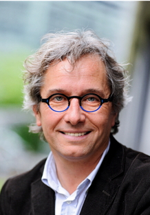
Dr. Jean-Michel Gerard
Self-assembled quantum dots, from a discovery by chance to key applications in quantum photonics
In November 1984, researchers from the France Telecom R&D Labs (“CNET”) discovered by chance a way to build In-rich clusters in GaAs that were both dislocation-free and optically-efficient, when exploring the growth of highly strained InAs/GaAs superlattices by molecular beam epitaxy [1]. They quickly realized the strong interest of such objects for studying the intrinsic properties of OD semiconductor nanostructures. However, it was by then far from clear that such objects, today known as self-assembled quantum dots (QDs), could be fabricated in a reproducible way and would actually behave as quantum dots. Additionally, the broad emission line observed for In-rich cluster ensembles seemed to preclude practical applications in optoelectronics (e.g. to realize the Arakawa-Sakaki QD laser proposal).
Having worked at CNET on InAs/GaAs highly strained superlattices and QDs from 1986 to 2001, I will give a personal view on several experiments which have contributed to unveil the strong assets of self-assembled QDs for optoelectronics and quantum photonics.
I will first recall how optical studies have brought in 92-93 essential insights on the nucleation and growth of InAs islands on GaAs, and unveiled a key role of growth dynamics (growth rate, growth interruptions) on the final size of buried In-rich clusters, in marked contrast with quantum wells [2]. Reproducible fabrication of self-assembled InAs “quantum boxes”, as we called these nanostructures by then, was fully mastered at CNET as of 1992.
I will also put into context the first optical experiment on single self-assembled QDs, isolated in etched mesa structures [3]. The observation of “narrow lines” for single QDs at low temperature opened the way to the amazing blossoming of single QD spectroscopy worldwide. Nowadays, the properties of these “artificial atoms”, including perturbations induced by their solid-state environment, are known with exquisite detail.
The observation of atomic-like properties for QDs was also a strong incentive to explore their potential interest for quantum optics. We started in 1995 to insert InAs QDs in microcavities, in an attempt to explore and exploit cavity quantum electrodynamics effects (CQED). Following the observation of the Purcell effect [4], we have proposed [5] and demonstrated [6] a first single-mode single photon source, that harnesses the emission of a single QD in a pillar microcavity [5]. This device belongs to a novel generation of CQED optoelectronic devices, that is poised to become an essential resource for quantum photonics.
References
[1] L. Goldstein, F. Glas, J.Y. Marzin, M.N. Charasse, G. LeRoux, Appl. Phys. Lett. 47, 1099 (1985)
[2] Result first presented at the NATO ASI school “Confined electrons and Photons”, Erice, July 1993;
J.M. Gérard, NATO ASI series B340, 357, Plenum (1995); J. Crys. Growth 150, 351 (1995)
[3] J.Y. Marzin, J.M. Gérard, A. Izraël, D. Barrier and G. Bastard, Phys. Rev. Lett. 73, 716 (1994)
[4] J.M. Gérard, B. Sermage, B. Gayral, E. Costard, V. Thierry-Mieg, Phys. Rev. Lett. 81, 1110 (1998)
[5] J.M. Gérard and B. Gayral, IEEE-J. Lightwave Technol. 17, 2089 (1999)
[6] E. Moreau, I. Robert, J.M. Gérard, I. Abram, L. Manin and V. Thierry-Mieg, APL79, 2865 (2001)
Biography:
Jean-Michel Gérard has received his PhD (1990) from Paris VI University for a thesis entitled “Growth by molecular beam epitaxy of highly-strained InAs/GaAs semiconductor heterostructures and optical study of their electronic properties”. From 1986 to 2001, he was Engineer of the French Ministry of Defense performing research within France Telecom R&D laboratories, in charge of research activities on quantum dots (QDs) from 1995 on. He joined the French Atomic Commission (CEA) laboratories in Grenoble in 2001, was head of the CEA-CNRS Nanophysics and Semiconductors joint laboratory (01-05), of the Physics of Materials and Microstructures Laboratory (SP2M) of CEA and University Joseph Fourier (06-15), and Founding Director of the Quantum Photonics, Electronics and Engineering Laboratory (PHELIQS) of CEA and University Grenoble Alpes.
Between 1986 and 1995, he has given pioneering contributions to the growth of III-V nanostructures (growth of InAs/GaAs short-period superlattices, investigation of segregation effects at the monolayer scale, control of QDs self-assembling). In 1994, he initiated with J.Y. Marzin optical studies on single self-assembled QDs, isolated from dense ensembles. He has unveiled the strong potential of these “artificial atoms” for quantum electrodynamics experiments in solid-state microcavities (1998) and photonic waveguides (2010). He introduced in 1998 the widely-used protocol harnessing radiative cascades in a single QD to generate single photons on demand and demonstrated in 2001 the first single-mode single photon source, based on a single QD in a micropillar cavity. Among other distinctions, he has received the Léon Brillouin Great Prize of the French Optical Society in 2016 and the Welker Award in 2024.
Email:
Address:Laboratoire PHELIQS (Photonique, Electronique et Ingénierie Quantiques) de la Direction de la Recherche CEA, 17 avenue des Martyrs, Grenoble, France, 38000
Agenda
Agenda
14:00 - 15:00 - Professor Claude Weisbuch (IP Paris & UC Santa Barbara, USA)
Keynote Lecture: The long saga of quantum size effects in semiconductors and of their applications: From quantum dots to quantum wells, … back to quantum dots
15:00 - 15:30 - Break
15:30 - 16:30 - Dr. Jean-Michel Gérard (CEA LETI)
Keynote Lecture: Self-assembled quantum dots, from a discovery by chance to key applications in quantum photonics
16:40 - 17:10 - Round Table Discussion
Challenges and Future Perspectives in Quantum Dot Research
17:15 - 18:15 - Cocktail Reception, Networking and Discussion


