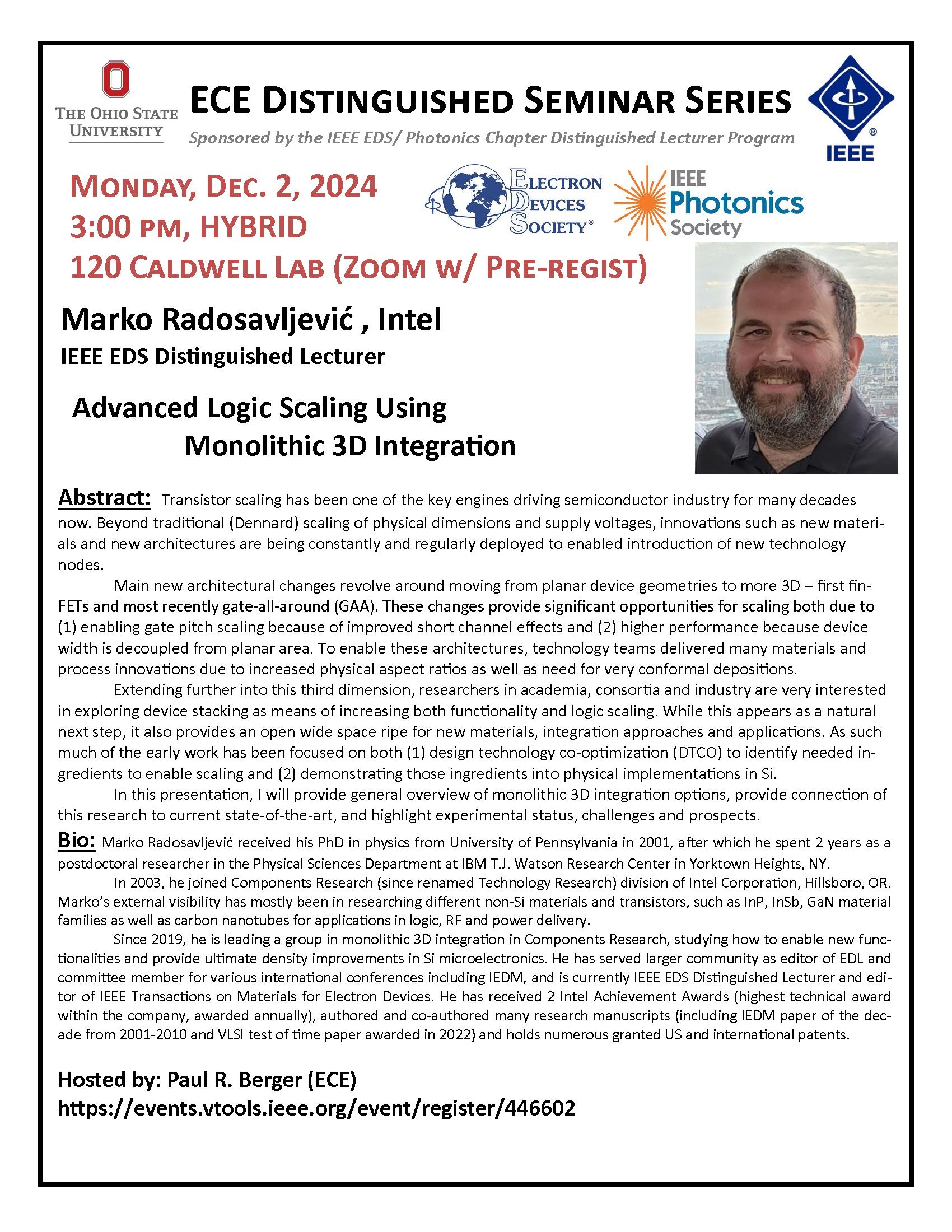
IEEE EDS/PHO Columbus DL Speaker: Advanced Logic Scaling Using Monolithic 3D Integration
Date and Time
Location
Hosts
Registration
-
 Add Event to Calendar
Loading virtual attendance info...
Speakers
Marko Radosavljević of Intel
Advanced Logic Scaling Using Monolithic 3D Integration
Abstract: Transistor scaling has been one of the key engines driving semiconductor industry for many decades now. Beyond traditional (Dennard) scaling of physical dimensions and supply voltages, innovations such as new materials and new architectures are being constantly and regularly deployed to enabled introduction of new technology nodes.
Main new architectural changes revolve around moving from planar device geometries to more 3D – first finFETs and most recently gate-all-around (GAA). These changes provide significant opportunities for scaling both due to (1) enabling gate pitch scaling because of improved short channel effects and (2) higher performance because device width is decoupled from planar area. To enable these architectures, technology teams delivered many materials and process innovations due to increased physical aspect ratios as well as need for very conformal depositions.
Extending further into this third dimension, researchers in academia, consortia and industry are very interested in exploring device stacking as means of increasing both functionality and logic scaling. While this appears as a natural next step, it also provides an open wide space ripe for new materials, integration approaches and applications. As such much of the early work has been focused on both (1) design technology co-optimization (DTCO) to identify needed ingredients to enable scaling and (2) demonstrating those ingredients into physical implementations in Si.
In this presentation, I will provide general overview of monolithic 3D integration options, provide connection of this research to current state-of-the-art, and highlight experimental status, challenges and prospects.
Biography:
Bio: Marko Radosavljević received his PhD in physics from University of Pennsylvania in 2001, after which he spent 2 years as a postdoctoral researcher in the Physical Sciences Department at IBM T.J. Watson Research Center in Yorktown Heights, NY.
In 2003, he joined Components Research (since renamed Technology Research) division of Intel Corporation, Hillsboro, OR. Marko’s external visibility has mostly been in researching different non-Si materials and transistors, such as InP, InSb, GaN material families as well as carbon nanotubes for applications in logic, RF and power delivery.
Since 2019, he is leading a group in monolithic 3D integration in Components Research, studying how to enable new functionalities and provide ultimate density improvements in Si microelectronics. He has served larger community as editor of EDL and committee member for various international conferences including IEDM, and is currently IEEE EDS Distinguished Lecturer and editor of IEEE Transactions on Materials for Electron Devices. He has received 2 Intel Achievement Awards (highest technical award within the company, awarded annually), authored and co-authored many research manuscripts (including IEDM paper of the decade from 2001-2010 and VLSI test of time paper awarded in 2022) and holds numerous granted US and international patents.
Address:United States


