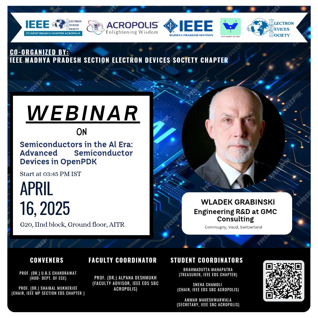
Technical Talk "Semiconductor in the AI Era: Advanced Semiconductor Devices in Open PDK."
AITR Indore MP India
AI-Driven Semiconductor Design
AI is revolutionizing semiconductor design by automating complex tasks, optimizing performance metrics, and accelerating time-to-market. Tools like Synopsys.ai offer AI-driven solutions across the entire design flow, enhancing power, performance, and area (PPA) outcomes.
2. Open PDKs and Collaborative Innovation
Open PDKs, such as those provided by SkyWater and initiatives like Efabless, democratize access to semiconductor design, allowing a broader range of innovators to participate. These open-source frameworks facilitate collaborative development and rapid prototyping.
3. Advanced Semiconductor Devices for AI
The AI era demands advanced semiconductor devices capable of handling intensive computations. Innovations in 2.5D and 3D packaging, high-bandwidth memory (HBM), and chiplet-based architectures are critical to meet these requirements.
Date and Time
Location
Hosts
Registration
-
 Add Event to Calendar
Loading virtual attendance info...
- Contact Event Host
-
- Co-sponsored by IEEE EDS SB Chapter Acropolis , IEEE EDS MP Section and VLSI Society of India
- Starts 09 April 2025 06:30 PM UTC
- Ends 16 April 2025 06:30 AM UTC
- No Admission Charge
Speakers
Mr. Wlaked Grabinski of R & D GMC Consulting
Semiconductor in the AI Era: Advanced Semiconductor Devices in Open PDK
The topic "Semiconductor in the AI Era: Advanced Semiconductor Devices in Open PDK" explores the convergence of artificial intelligence (AI) and semiconductor technology, particularly focusing on the development and utilization of advanced semiconductor devices within open Process Design Kits (PDKs).
Email:
Address:Vaud , Switzerland, Vaud, Switzerland
IEEE EDS SB Chapter Indore and IEEE EDS MP Section