IEEE SSCS Oregon Chapter May Meeting and Seminar (In-Person)
IEEE SSCS Oregon Chapter May Meeting and Seminar
Join us for a talk from SSCS Distinguished Lecturer Dr. Alvin Loke from Intel, San Diego, on Tuesday, May 6th, 2025. The seminar will be held from 5:30pm to 7:30pm (PST) in-person. Food and drinks will be provided.
Topic:
The Road to Gate-All-Around CMOS
Abstract:
Despite the much debated end of Moore's Law, CMOS scaling still maintains economic relevance with 3nm finFET SoCs already in the marketplace for three years and 2nm gate-all-around SoCs anticipated late this year. Area scaling extensively driven by design/technology innovations co-optimized for primarily logic scaling continue to offer compelling node-to-node power, performance, area, and cost benefits. In this tutorial, we will start with a walk through memory lane, recounting a brief history of transistor evolution to motivate the migration from the planar MOSFET to the fully depleted FinFET. We will summarize the key process technology elements that have enabled the finFET CMOS nodes, highlighting the resulting device technology characteristics and challenges. This will set the context for motivating the transition to the gate-all-around device architecture, namely nanoribbons or nanosheets, and unveiling the magic of how these devices are fabricated.
Speaker Biography:
Alvin Loke is a Senior Principal Engineer at Intel, San Diego, working on analog design/technology co-optimization for Intel’s gate-all-around CMOS. He has previously worked on CMOS nodes spanning 250nm to 2nm at Agilent, AMD, Qualcomm, TSMC, and NXP. Alvin received a BASc from the University of British Columbia, and MS and PhD from Stanford. After several years in CMOS process integration, he has since worked on analog/mixed-signal design focusing on a variety of wireline links including chiplet IOs, design/model/technology interface, and analog design methodologies. Alvin has been an active IEEE Solid-State Circuits Society (SSCS) volunteer since 2003, having served as Distinguished Lecturer, AdCom Member, CICC Committee Member, Webinar Chair, Denver and San Diego Chapter Chair, as well as JSSC, SSCL, and Solid-State Circuits Magazine Guest Editor. He currently serves as the VLSI Symposium Secretary and SSCS Global Chapters Chair. Alvin frequently speaks on CMOS technology and its impact on analog design, having authored invited publications including the CICC 2018 Best Paper and short courses at ISSCC, VLSI Symposium, CICC, and BCICTS.
Date and Time
Location
Hosts
Registration
-
 Add Event to Calendar
- 2501 NW 229th Avenue
- Hillsboro, Oregon
- United States 97124
- Building: Intel Ronler Acres
- Room Number: RA1 Auditorium
Speakers
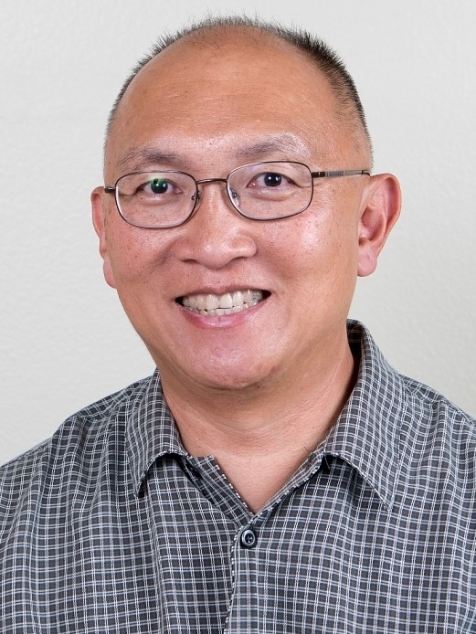
Dr. Alvin Loke of Intel
The Road to Gate-All-Around CMOS
Despite the much debated end of Moore's Law, CMOS scaling still maintains economic relevance with 3nm finFET SoCs already in the marketplace for three years and 2nm gate-all-around SoCs anticipated late this year. Area scaling extensively driven by design/technology innovations co-optimized for primarily logic scaling continue to offer compelling node-to-node power, performance, area, and cost benefits. In this tutorial, we will start with a walk through memory lane, recounting a brief history of transistor evolution to motivate the migration from the planar MOSFET to the fully depleted FinFET. We will summarize the key process technology elements that have enabled the finFET CMOS nodes, highlighting the resulting device technology characteristics and challenges. This will set the context for motivating the transition to the gate-all-around device architecture, namely nanoribbons or nanosheets, and unveiling the magic of how these devices are fabricated.
Biography:
Alvin Loke is a Senior Principal Engineer at Intel, San Diego, working on analog design/technology co-optimization for Intel’s gate-all-around CMOS. He has previously worked on CMOS nodes spanning 250nm to 2nm at Agilent, AMD, Qualcomm, TSMC, and NXP. Alvin received a BASc from the University of British Columbia, and MS and PhD from Stanford. After several years in CMOS process integration, he has since worked on analog/mixed-signal design focusing on a variety of wireline links including chiplet IOs, design/model/technology interface, and analog design methodologies. Alvin has been an active IEEE Solid-State Circuits Society (SSCS) volunteer since 2003, having served as Distinguished Lecturer, AdCom Member, CICC Committee Member, Webinar Chair, Denver and San Diego Chapter Chair, as well as JSSC, SSCL, and Solid-State Circuits Magazine Guest Editor. He currently serves as the VLSI Symposium Secretary and SSCS Global Chapters Chair. Alvin frequently speaks on CMOS technology and its impact on analog design, having authored invited publications including the CICC 2018 Best Paper and short courses at ISSCC, VLSI Symposium, CICC, and BCICTS.
Agenda
5:30pm - 7:30pm: Professional/Career Seminar
Media
| Group Photo | 186.04 KiB | |
| Speaker Gift | 148.66 KiB |

