Measurement of Wide Bandgap Power Devices
IEEE North Jersey Section Co-Sponsors the Talk: "Measurement of Wide Bandgap Power Devices"
This webinar addresses the measurement of Wide-Bandgap (WBG) power devices. It provides practical techniques specifically designed for engineers with advanced semiconductor technologies, including Gallium Nitride (GaN) and Silicon Carbide (SiC). As these technologies advance the field of energy conversion by facilitating higher switching frequencies and decreasing power losses, they introduce distinct measurement challenges that necessitate specialized knowledge. The critical skills discussed in this webinar encompass the selection of high-bandwidth differential voltage probes, properly de-skewing voltage and current measurements, identifying and mitigating parasitics, and applying best practices to obtain clean and reliable data for WBG designs.
Date and Time
Location
Hosts
Registration
-
 Add Event to Calendar
Loading virtual attendance info...
- Contact Event Host
-
Ajay Poddar (akpoddar@ieee.org), Edip Niver (edip.niver@njit.edu), Durga Mishra (dmisra@njit.edu), (Anisha Apte (anisha_apte@ieee.org)
- Co-sponsored by IEEE North Jersey Section
Speakers
Marcus Sonst of Rohde & Schwarz
Measurement of Wide Bandgap Power Devices
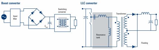
One of the most significant challenges in contemporary power electronics is testing systems that utilize wide bandgap (WBG) semiconductors, such as silicon carbide (SiC) and gallium nitride (GaN). The integration of these materials into power devices, like converters, leads to higher operating frequencies, voltages, and temperatures. This results in numerous advantages in converter design, including improved power efficiency, reduced size and weight, and lower manufacturing costs. WBG materials have been adopted in specific applications where power density and size are critical, such as solar energy systems, electric vehicles (EVs), EV chargers, and consumer electronics.
Despite the numerous benefits that SiC and GaN provide, it's essential to recognize the unique challenges faced when testing circuits that utilize these technologies:
- **Electromagnetic Interference:** Higher switching frequencies, steeper edges, and elevated voltages generate more frequency harmonics due to increased overshoots and ringing. Consequently, higher levels of conducted and radiated emissions are expected in converter designs.
- **Parasitics:** At elevated frequencies, the parasitic behavior of passive components can adversely affect the performance of a power device. Therefore, proper identification and management of these parasites are crucial.
- **Dynamic Range:** Power electronics devices operate across wide ranges of current and voltage, which can complicate accurate measurements.
Quantification of Losses:** Fast slew rates create challenges when estimating transistor switching losses. Factors such as parasitics, propagation delays, and the bandwidth of the test and measurement equipment can influence the accuracy of loss calculations.
In addition to these new challenges presented by the use of WBG materials, design engineers conduct various tests to verify and validate a power device as a switched-mode power supply (SMPS). These tests include assessments of efficiency, ripple, start-up and shut-down behavior, power quality, inrush currents, input harmonics, simulations of real-life scenarios (e.g., battery cells in an EV), stability, and more.
Furthermore, engineers engage in detailed battery modeling and simulations, which are essential for predicting battery performance and lifespan in practical applications. Such simulations provide valuable data for optimizing battery designs and developing efficient battery management systems (BMS). Likewise, monitoring a device’s power consumption is crucial throughout the development process. This information is vital for evaluating device efficiency and ensuring regulatory compliance. Each of these tests presents its own challenges and necessitates appropriate test and measurement equipment to obtain precise and reliable results at all stages of the design process, from debugging prototypes to validating the SMPS.
Biography: