A Unified Compact Model for GaN-Based HEMTs
III-V channel field-effect transistors (FETs), such as GaN-based high electron-mobility transistors (HEMTs), have emerged as promising candidates for future generation high-frequency, high-voltage, and high-power ULSI applications. Development of a compact model for HEMTs in III-V/Si co-integrated hybrid circuit design is becoming an urgent need for semiconductor industry. This talk presents a unified compact model for generic GaN-based HEMTs, which has been validated with the exact numerical solutions for a wide range of device parameters and verified with experimental data of sub-100-nm gate lengths. The model is based on unified regional modeling (URM) of the 2-dimensional electron gas (2DEG) charge density, including the two lowest subbands of the triangular well in the active region, and extending to the moderate-inversion and subthreshold regions of operation in a single-piece formulation. The 2DEG charge density model is adopted in the surface-potential (SP)-based model for conventional bulk/SOI/multigate MOSFETs, which makes it compatible and scalable for future III-V/Si co-integrated generations. In this talk, fundamentals in compact modeling of generic FETs are reviewed in the context of the URM approach, and its extension to modeling the 2DEG in HEMT devices, including charge-based model for intrinsic as well as parasitic capacitances for high-frequency applications. HEMT-specific features will also be discussed, such as source/drain access resistances, current-collapse, self-heating, and parallel-channel effects. Model comparisons with quasi-ballistic (QB)-based formalism will be made, and model implementation in SPICE as well as application to high-frequency digital/analog circuit building blocks will be demonstrated.
Date and Time
Location
Hosts
Registration
-
 Add Event to Calendar
- 141 Warren St
- Newark, New Jersey
- United States 07102
- Building: Electrical and Computer Engineering Center
- Room Number: 202
- Click here for Map
- Contact Event Host
- Durga Misra, ECE Dept, NJIT, (973) 596-5739, email: dmisra@njit.edu, Edip Niver, ECE Dept, NJIT, (973) 596-3542, Email: edip.niver@njit.edu
- Co-sponsored by ECE Dept, NJIT, ED/CAS, MTT/AP
Speakers
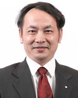
 Xing Zhou of School of Electrical and Electronic Engineering Nanyang Technological University Singapore
A Unified Compact Model for GaN-Based HEMTs
III-V channel field-effect transistors (FETs), such as GaN-based high electron-mobility transistors (HEMTs), have emerged as promising candidates for future generation high-frequency, high-voltage, and high-power ULSI applications. Development of a compact model for HEMTs in III-V/Si co-integrated hybrid circuit design is becoming an urgent need for semiconductor industry. This talk presents a unified compact model for generic GaN-based HEMTs, which has been validated with the exact numerical solutions for a wide range of device parameters and verified with experimental data of sub-100-nm gate lengths. The model is based on unified regional modeling (URM) of the 2-dimensional electron gas (2DEG) charge density, including the two lowest subbands of the triangular well in the active region, and extending to the moderate-inversion and subthreshold regions of operation in a single-piece formulation. The 2DEG charge density model is adopted in the surface-potential (SP)-based model for conventional bulk/SOI/multigate MOSFETs, which makes it compatible and scalable for future III-V/Si co-integrated generations. In this talk, fundamentals in compact modeling of generic FETs are reviewed in the context of the URM approach, and its extension to modeling the 2DEG in HEMT devices, including charge-based model for intrinsic as well as parasitic capacitances for high-frequency applications. HEMT-specific features will also be discussed, such as source/drain access resistances, current-collapse, self-heating, and parallel-channel effects. Model comparisons with quasi-ballistic (QB)-based formalism will be made, and model implementation in SPICE as well as application to high-frequency digital/analog circuit building blocks will be demonstrated.
Biography:
Dr. Xing Zhou received the B.E. degree from Tsinghua University, China in 1983, and the M.S. and Ph.D. degrees in electrical engineering from the University of Rochester, NY, USA in 1987 and 1990, respectively.
He joined the faculty of the School of Electrical and Electronic Engineering, Nanyang Technological University in 1992. His past research interests include Monte Carlo simulation of photocarrier transport and ultrafast phenomena as well as mixed-mode circuit simulation and CAD tool development. His current research focuses on the development of compact models for circuit simulation for conventional (bulk/SOI) and emerging (double-gate/nanowire) nanoscale-CMOS as well as III-V/GaN-based HEMT devices. He was visiting professor to Stanford University (1997/2001), Hiroshima University (2003), Universiti Teknologi Malaysia (2007), Fudan University (2011/2012), and Tokyo Institute of Technology (2011/2012). He is the founding chair of the Workshop on Compact Modeling (WCM) in association with the Nano Science and Technology Institute Nanotech Conference since 2002. He was guest editor-in-chief for the special issue on compact modeling of emerging devices for the IEEE Transactions on Electron Devices (Feb. 2014 issue). He has served as an IEEE Electron Devices Society (EDS) distinguished lecturer since 2000, and he has given ~140 lectures and invited talks around the world. Dr. Zhou is currently EDS vice-president for regions/chapters, an elected member-at-large of the EDS Board of Governors, and editor for the IEEE Electron Device Letters.
Email:
Address:Associate Professor, Division of Microelectronics, School of Electrical & Electronic Engineering, Nanyang Technological University, Singapore 639798, Singapore, 639798
Xing Zhou of School of Electrical and Electronic Engineering Nanyang Technological University Singapore
A Unified Compact Model for GaN-Based HEMTs
Biography:
Email:
Address:Singapore 639798, Singapore
Xing Zhou of School of Electrical and Electronic Engineering Nanyang Technological University Singapore
A Unified Compact Model for GaN-Based HEMTs
Biography:
Email:
Address:Singapore 639798, Singapore
Agenda
5-6 PM DL Talk
ECEC-Room 202
All Welcome: You don't have to be an IEEE Member to attend.
