43rd IEEE EDS Activities in Western New York Conference
MEETING ANNOUNCEMENT & CALL FOR POSTERS
Thursday, November 7, 2019
University Gallery
James E. Booth Hall (Building 7A)
Rochester Institute of Technology
Rochester, NY
The focus of this conference is to bring engineers and researchers together to share information on a wide variety of topics related to microelectronic devices and systems. The conference will be a joint event technically co-sponsored by the Electron Devices Society and the Photonics Society of the IEEE Rochester Section. The conference will be held at RIT in the University Gallery in Booth Hall; please visit the following link: https://maps.rit.edu/
The conference agenda will begin at 9 AM, and the first invited presentation will follow opening remarks at 9:40 AM. There are six invited talks separated by lunch and an afternoon coffee break. Student presenters will showcase their work at poster sessions during the lunch and reception following the technical presentations.
See Full Agenda Below
Invited Speakers: See details below
We are exceedingly pleased to have the following invited speakers for this event.
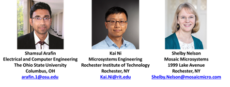
Prof. Shamsul Arafin, The Ohio State University, “Compound III-V Semiconductor based Classical and Non-Classical Light Emitters at Visible through Mid-Infrared”
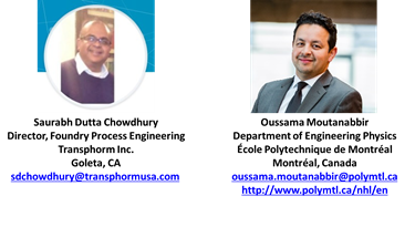
Prof. Oussama Moutanabbir, Ecole Polytechnique de Montreal, “Silicon-Integrated Quantum Electronics and Photonics”
Adam Milton, Director, Mohawk Valley Fab, Cree, Inc., “Cree Wolfspeed SiC Technology: Innovation today, powering the future”
Dr. Saurabh Chowdhury, Director, Foundry Process Engineering, Transphorm Inc., “650V GaN HEMT: Manufacturing and Scaling”
Dr. Shelby Nelson, Mosaic Microsystems, "Thin Glass Substrates for Advanced Packaging Applications"
Prof. Kai Ni, Rochester Institute of Technology, “Ferroelectronics: From Memory to Computing”
Call for Posters:
Abstracts are being solicited for poster presentations in microelectronics and photonics, especially those which promote research and development activity in Western New York. Abstracts must be received by Nov 4th. Submission can be done electronically to the host emails using MS‑Word or pdf formats.
Register Now!
Date and Time
Location
Hosts
Registration
-
 Add Event to Calendar
- Rochester Institute of Technology
- University Gallery
- Rochester, New York
- United States 14623
- Building: Booth Hall (7A)
- Click here for Map
- Contact Event Host
-
EDS Conference co-chairs:
Karl D. Hirschman, Electrical & Microelectronic Engineering kdhemc@rit.edu
Parsian K. Mohseni, Microsystems Engineering pkmeen@rit.edu
Rochester Institute of Technology
- Co-sponsored by CH01214 - Rochester Section Chapter,PHO36
- Starts 01 October 2019 11:00 AM UTC
- Ends 08 November 2019 05:00 AM UTC
- No Admission Charge
Speakers
 .
.
Oussama Moutanabbir
Silicon-Integrated Quantum Electronics and Photonics
Abstract:
For decades, compound semiconductors have been successfully used for a precise and simultaneous control of lattice parameters and bandgap structures bringing to existence a variety of functional heterostructures and low-dimensional systems. Extending this paradigm to group IV semiconductors will be a true breakthrough that will pave the way for scalable, compact, and silicon-compatible optoelectronic, photonic, and quantum devices. With this perspective, I will describe strategies and new material systems to independently engineer lattice dynamics and band structure in group IV semiconductors. The materials to be discussed are grown epitaxially using chemical vapor deposition system equipped with isotopically enriched precursors with purity higher than 99.9%: 28SiH4, 29SiH4, 30SiH4, 74GeH4, and 76GeH4 in addition to Sn precursors. I will address the epitaxial growth of (Si)GeSn semiconductors and their relevance for Si-based mid-infrared photonics and quantum computing. I will also describe our progress in the use of stable isotopes as an additional degree of freedom in the growth of semiconductor quantum structures. This isotope engineering provides a wealth of opportunities to manipulate their basic properties, design an entirely new class of devices, and highlight subtle but important fundamental processes.
Bio:
Oussama Moutanabbir is a Professor holding a Canada Research Chair in Nano and Quantum Semiconductors at the department of Engineering Physics of École Polytechnique de Montréal (Canada). As a follow of Japan Society of the Promotion of Science, he worked at the Quantum Computing Lab at Keio University (Japan) and before taking position in Montreal, he was a Project Leader at the Max Planck Institute of Microstructure Physics (Germany). He also held a joint appointment as an Invited Researcher at RIKEN Institute of Advanced Science (Japan) between 2009 and 2015. His research is in materials physics and engineering encompassing fundamental scientific and industrial activities. His main work focuses on expanding the fundamental understanding of basic physical properties of a variety of group IV nanomaterials and quantum structures. Additionally, his group also made significant contributions leading to commercial products through numerous joint collaborations with high-tech companies focusing primarily on large-scale integration processes for sensing, imaging, optoelectronic, photovoltaic, and electronic applications. For instance, his recent project with Teldyne-Dalsa has led to the commercialization in 2018 of the first made-in-Canada uncooled thermal and infrared cameras. This project was awarded the ADRIQ’s Innovation Award, the ADRIQ’s Partnership Award, and the 2019 NSERC’s Synergy Award.
Saurabh Dutta Chowdhury
The Role of UCSB Nanolab in accelerating the Commercialization of 650V GaN-on-Si HEMTs at Transphorm based in Goleta,CA : Lessons for RIT to leverage thirty year strength in Microelectronics for the Upstate NY region based startups
Abstract:
This talk illustrates how GaN-on-Si technology was developed and then rolled out in collaboration with academia for the world’s first highly reliable 650V GaN HEMT [2,3,4,5,6,7,8] by demonstrating three years of manufacturing data of since ramp. This technology was initially developed in a pilot line in Transphorm Goleta, CA and then later ported into a Si-CMOS compatible 6-inch foundry at AFSW(Aizu Fujitsu Semiconductor Wafers Solution Ltd). Data set generated from over three thousand wafers worth of data spread over three generations of technology nodes covering multiple products and packages post qualification is presented Silicon manufacturing processes are employed including gold-free, and avoiding the use of evaporation/liftoff typical to compound semiconductors. Best practice of defect detection, failure analysis and process control methods from Si manufacturing industry have been employed to maintain and improve yield for this new technology. Probe yield and line yield for the GaN process now matches that of mature Si-CMOS process running in the same fabrication facilityWide bandgap high-speed and high- voltage GaN devices significantly reduce the system size and improve energy efficiency of power conversion in all areas of electricity conversion, ranging from PV inverters to electric vehicles. The results below demonstrates that GaN high volume production is now a reality. This is the current third stage of Transphorm funded by Series C and D investment led by KKR and one other strategic European IDM. However, prior to this phase of mass production since 2015 there were two earlier phases described below which may be relevant for RIT.
Bio:
Seasoned manager with over twenty years of yield enhancement, technology development, operations, and business development experience in the semiconductor wafer fabrication and equipment industry. He has broad experience of technology development and transfer to manufacturing spanning Fortune 500 companies Applied Materials, Cypress Semi and Maxim Integrated products rising through the ranks to functional management role during his first fifteen years since RIT. He started his industrial career at Applied Materials in the area of Dry Etch as an applications engineer between 1995-2000. Thereafter he joined Cypress San Jose R&D Fab developing Dry Etch processes for 90 and 65 nm SRAMs at Cypress transferred to Minnesota Production fab. His first Operations Management role was at Maxim Dallas where he ran the Photo/Etch group -Process and Equipment engineers for a 24x7 fab producing 3000 + wafers per month for 0.35 um BiCMOS and Analog/Mixed Signal power management products. Since 2011, he has been with a KKR backed Santa Barbara based startup Transphorm developing wide bandgap GaN based IC for efficient and compact charging solutions aimed at electric car on board charger, server power supply, PV inverter and Servo motor driver applications. At Transphorm, he runs all of front end manufacturing working across functional environments interacting with device, integration, module, packaging and equipment teams spanning Santa Barbara, Aizu Wakamatsu Japan, Hsinchu Taiwan and Penang Malaysia. During this period Transphorm moved from Series B to Series D funding graduating from the backing of Sand hill road early investors like Kleiner Perkins, Lux Capital and Google Ventures to late stage investors like KKR, the Japanese Sovereign Wealth fund INCJ and a large unnamed strategic chip company. All of this has been possible because Transphorm IC chips are now in mass production and doing well in field trials at strategic customers. One key accomplishment led by Saurabh was the development of industrial scale supply chain with Fujitsu as JV partner for front end manufacturing enabling laboratory scale technology developed at UCSB Umesh Mishra lab to move to mass manufacturing in Fujitsu Foundry. He holds a Masters in Engineering from Rochester Institute of Technology -Microelectronics Engineering'94 on a SRC funded full fellowship. Maxim integrated sponsored him to Harvard Business School - Program for Leadership Development in 2007-08.
 .
.
Shamsul Arafin
Compound III-V Semiconductor based Classical and Non-Classical Light Emitters at Visible through Mid-Infrared
Abstract:
III-V compound semiconductor materials and photonic devices are expected to play an important role in addressing ongoing and future challenges in the field of communication and sensing. Ultra high-speed, short and long-range communication links; portable and power-efficient computing devices; solid-state lighting; ultra-fast interconnects; and high-performance optical sensors in sensing applications are critically depending on the success of next-generation emerging semiconductor materials and the resulting photonic devices. In this talk, I will mainly discuss about recent cutting-edge research efforts made by my team at OSU on III-V semiconductor materials and photonic devices. In particular, an emphasis will be given on nitride-based electrically-pumped lasers with emission wavelengths of the ultraviolet and blue regions. Design, fabrication and testing results of such lasers will also be presented here. In addition, I will present the recent theoretical and experimental results of advanced antimonide-based lasers, being useful for sensing and defense applications. Considering a significant promise of quantum technologies, I will also briefly show how my research enters into the quantum territory for developing non-classical devices including single photon emitters that could enable robust communication-based applications, such as electronic warfare, signal intelligence, and counter-digital radio frequency memory.
Bio:
Dr. Shamsul Arafin is an Assistant Professor in the Electrical and Computer Engineering Department at The Ohio State University. Prior to joining OSU, he worked as a Project Scientist in the Department of Electrical and Computer Engineering at the University of California at Santa Barbara (UCSB), USA. He received the B.Sc. degree in Electrical and Electronics Engineering from Bangladesh University of Engineering and Technology (BUET), Bangladesh in 2005 and the M.Sc. degree in Communication Technology from Universität Ulm, Germany, in 2008. He received his Ph.D. degree from Technische Universität München, Walter Schottky Institut Germany in 2012. He then joined the Nanophotonics Group of Electrical and Computer Engineering Department at McGill University as a post-doctoral fellow. He also worked as a Postdoctoral Research Scholar in the Department of Electrical Engineering at the University of California at Los Angeles, CA, USA.
Kai Ni
Ferroelectronics: From Memory to Computing
Abstract:
Research discovery of ferroelectricity in doped hafnium dioxide thin films has ignited tremendous activity in exploration of ferroelectric FETs for a range of applications from low-power logic to embedded non-volatile memory and to novel computing paradigms. In this talk, key milestones in the evolution of Ferroelectric Field Effect Transistors (FeFETs) and the emergence of a versatile ferroelectronic platform are presented. FeFET exhibits superior energy efficiency and high performance as embedded nonvolatile memory. When embedded into logic, such as SRAM or D-flip-flop, nonvolatile processor can be designed, which is critical for intermittent computing with unreliable power. The partial polarization switching in multi-domain ferroelectric can be harnessed to develop analog synaptic weight cell for deep learning accelerators. To further improve the energy-efficiency of computation, ferroelectric in-memory computing hardware primitive is designed, with one prominent example of ferroelectric TCAM. Utilizing the ferroelectric switching dynamics, ferroelectric neuron with intrinsic homeostasis can be realized to enable a unified ferroelectric platform for spiking neural network. From all these developments, ferroelectric emerges as a highly promising platform for various exciting applications.
Bio:
Kai Ni received the B.S. degree in Electrical Engineering from University of Science and Technology of China, Hefei, China in 2011, and Ph.D. degree of Electrical Engineering from Vanderbilt University, Nashville, TN, USA in 2016 by working on characterization, modeling, and reliability of III-V MOSFETs. Since then, he became a postdoctoral associate at University of Notre Dame, working on ferroelectric devices for nonvolatile memory and novel computing paradigms. He is now an assistant professor in Microsystems Engineering at Rochester Institute of Technology. He has around 60 publications in top journals and conference proceedings, including Nature Electronics, IEDM, VLSI Symposium, IRPS, EDL, etc. His current interests lie in nanoelectronic devices empowering unconventional computing, AI accelerator, security and memory technology.
Shelby Nelson
Thin Glass Substrates for Advanced Packaging Applications
Abstract:
Glass substrates with fine-pitch through-glass via (TGV) technology is a promising approach to system-in-a-package integration. Millimeter wave applications, in particular, benefit from the superior RF properties, dimensional stability, and surface properties of glass. Glass can be made in very thin sheets (<100 um) which aids in integration and eliminates the need for back-grinding operations. The biggest challenge to adopting glass as an advanced microelectronics packaging substrate is the existence of gaps in the supply chain, caused primarily by the difficulty in handling large, thin glass substrates using existing automation and processing equipment. This talk presents Mosaic Microsystem’s temporary bonding technology that allows the substrates to be processed in a semiconductor fab environment without the need to modify existing equipment. The technique allows the thin glass/silicon pair to be processed leveraging existing processes, with only a mechanical de-bond to yield finished substrates. The numerous benefits to this approach will be discussed.
Bio:
Shelby F. Nelson is the Chief Technology Officer of Mosaic Microsystems, a provider of glass-based advanced packaging solutions for electronic, photonic, and sensor products. Starting in late 2017, she has built the Mosaic technical team, and with them developed a cleanroom prototyping fab. Mosaic Microsystems has shipped hundreds of wafer products in the seven months since the fab came online. Shelby received the Ph.D. degree from Cornell University in Applied Physics. Since then she has studied silicon/germanium heterostructures at IBM’s Thomas J. Watson Research Center, pioneered organic electronics as the Clare Booth Luce Assistant/Associate Professor of Physics at Colby College, worked at Xerox Corporation as a semiconductor device physicist in ink jet, and been a senior research scientist in the Kodak Research Labs at Eastman Kodak, where she worked primarily on inorganic thin-film printed electronics. She has authored over 40 refereed journal articles and holds over 60 patents.
Agenda
9 AM Conference Registration & Continental Breakfast
9:40 AM Welcome & Opening Remarks
9:50 AM Shamsul Arafin, Electrical and Computer Engineering, The Ohio State University
“Compound III-V Semiconductor based Classical and Non-Classical Light Emitters at Visible through Mid-Infrared”
10:30 AM Coffee Break
10:50 AM Oussama Moutanabbir, Department of Engineering Physics, École Polytechnique de Montréal, Montréal, Canada
“Silicon-Integrated Quantum Electronics and Photonics”
11:30 AM “Nano-Flash” Poster Previews
12:00 PM Lunch & Poster Presentations
1 PM Adam Milton, Director, Mohawk Valley Fab, Cree, Inc., Marcy, NY
“Cree Wolfspeed SiC Technology: Innovation today, powering the future”
1:40 PM Saurabh Chowdhury, Director, Foundry Process Engineering, Transphorm Inc., Goleta, CA
“650V GaN HEMT: Manufacturing and Scaling”
2:20 PM Coffee Break
2:40 PM Shelby Nelson, Mosaic Microsystems, Rochester, NY
“Thin Glass Substrates for Advanced Packaging Applications”
3:20 PM Kai Ni, Microsystems Engineering, Rochester Institute of Technology
“Ferroelectronics: From Memory to Computing”
4:00 PM Closing Remarks
4 – 5 PM Poster Session Reception