Principles of Power Integrity for PDN Design
The PDN delivers power to the on-die CMOS circuits. CMOS circuits are sensitive to the power supply voltage because of Fmax, Vmin and Jitter considerations. Logic core speed is limited by the instantaneous power supply voltage including PDN voltage droops. The power supply voltage is often raised up to overcome PDN voltage droops to enable the on-die circuit voltage to stay above the minimum voltage (Vmin) where the circuits will run at rated clock speed (a high percentage of Fmax). These are the important PDN considerations for all CMOS circuits.
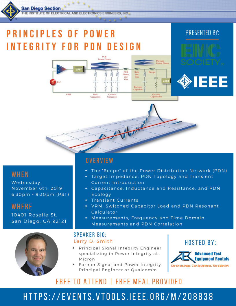
DC current is easy to deliver from the voltage regulator to the CMOS load and only suffers IR (current times resistance) loss. The major PDN problem is that current and power transients, associated with rapidly changing load conditions, demand a time varying amount current from the reactive (inductance and capacitance) nature of the PDN. Power integrity is all about managing the R, L and C properties of the PDN such that the transient currents can be delivered to the load with acceptable voltage droop. For IO circuits, the PDN properties are used to manage PDN induced jitter. All power supply design begins with the calculation of a target impedance, which is a strong indicator of the required PDN performance over a broad frequency range. It is used to manage PDN cost, performance and risk.
The PDN is designed and managed in the frequency domain where the goal is to manage R, L and C in a way that is close to the target impedance. A particular challenge is “Bandini Mountain” where the on-die capacitance and the bump loop inductance form an impedance peak that limits product performance and is expensive to fix. At the end of the day, all CMOS circuits function in the time domain. In the time domain, it is important to pay attention to the voltage responses from impulse, step and resonance current waveforms. They are intimately related to the frequency domain impedance profile and determine PDN costs, product power consumption and performance levels of the product.
Date and Time
Location
Hosts
Registration
-
 Add Event to Calendar
- Advanced Test Equipment Corp
- San Diego, California
- United States 92121
- Contact Event Host
- Co-sponsored by Yi Cao
- Starts 29 October 2019 05:00 PM UTC
- Ends 06 November 2019 09:00 PM UTC
- No Admission Charge
Speakers
Larry D Smith
Larry D. Smith is a Principal Signal Integrity engineer at Micron specializing in Power Integrity since August 2018. Prior to joining Micron, he was a PI engineer at Qualcomm in the mobile computing space beginning in 2011. He worked at Altera from 2005 to 2011 and Sun Microsystems from 1996 to 2005, where he did development work in the field of signal and power integrity. Before this, he worked at IBM in the areas of reliability, characterization, failure analysis, power supply and analog circuit design, packaging, and signal integrity. Mr. Smith received the BSEE degree from Rose-Hulman Institute of Technology and the MS degree in material science from the University of Vermont. He has more than a dozen patents and has authored numerous journal and conference papers. His most recent work is a book entitled “Principles of Power Integrity for PDN Design” published by Prentice Hall in 2017.
Agenda
6:00pm light snacks and networking
6:30pm Meeting/Presentation begins
8:30pm Adjourn
Free and dinner will be provided.