Lecture on "VLSI Design Flow (FPGA & ASIC)"
A session on the Design Flow in FPGA and ASIC was held on 17th of June, 2020 from 11AM - 1PM.
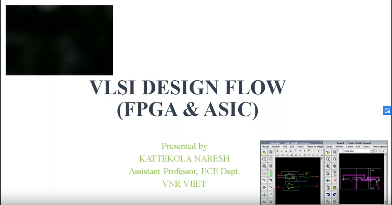
The entire design flow of ASIC and FPGA was thoroughly explained in this lecture by Mr K Naresh, Assistant Professor, Dept. of ECE, VNRVJIET.
The session started with the constraints and features one looks for while designing and manufacturing a chip few of which are cost, design time, component supply, prior experience, training, power source, power consumption, rapid prototyping, etc.
Classification and Comparison of VLSI CAD Tools was done, and step by step process was explained.
The meaning of technology and the actual meaning of channel length was explained, also the current technology was talked about.
Different tools which can be used for succesfully finishing a design flow was throwed light upon.
Date and Time
Location
Hosts
Registration
 Add Event to Calendar
Speakers
 Mr K Naresh of VNR Vignana Jyothi Institute of Engineering and Technology
VLSI Design Flow
Biography:
Assistant Professor, ECE Department
Teaching Interests: Switching Theory and Logic Design, Linear and Digital IC, VLSI Design, Digital design Through Verilog, Low Power VLSI design, Electronic Measurements and Instrumentation, CPLD & FPGA Architectures & Applications.
Email:
Agenda
The main aim of conducting this lecture was to familiarize the students with the ASIC & FPGA Design flow and build a strong understanding of the technical terms in the same process.
The lecture went smooth with the participants engaging with the speaker and asking doubts about confusing topics.
Media
| SS 1 | 531.90 KiB | |
| SS 2 | 539.58 KiB | |
| SS 3 | 615.24 KiB |