IEEE EDS Distinguished Lecture by Prof. Joachim N. Burghartz, IMS CHIPS, Stuttgart, Germany
IEEE EDS Distinguished Lecture by Prof. Prof. Joachim N. Burghartz, IMS CHIPS, Stuttgart, Germany
Talk: GaN-on-Si Technology for Power, RF & Specials
Date and Time
Location
Hosts
Registration
-
 Add Event to Calendar
Loading virtual attendance info...
- Dept. of ECE, NIT Silchar
- National Institute of Technology Silchar
- Silchar, Assam
- India 788010
- Building: ECE/CSE Building
- Room Number: EC-23
- Contact Event Hosts
- Co-sponsored by Dr. T. R. Lenka
Speakers
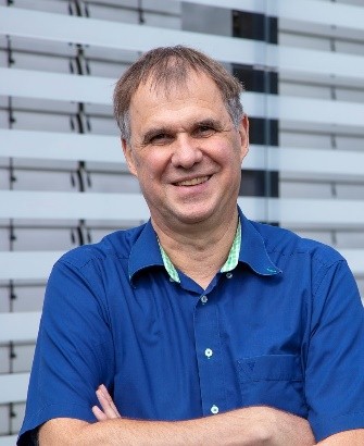
 Prof. Joachim N. Burghartz of Institut für Mikroelektronik Stuttgart, IMS CHIPS
GaN-on-Si Technology for Power, RF & Specials
Gallium-Nitride is a compound semiconductor material which provides an appealing alternative to the group-IV semiconductors Silicon and Silicon-Carbide for power, high-frequency/RF and special applications. It has the highest bandgap and provides the opportunity to engineer a two-dimensional electron gas (2DEG), thus featuring very high electron mobility. The allows for building a High-Electron-Mobility-Transistor (HEMT) on a semi-insulating substrate for applications to fast power switches, RF power transistors, and electronics used at unusually high temperatures and at high radiation. However, GaN has not yet conquered the electronics market due to the high cost and the sub-standard wafer substrate sizes when compared to Si. Also, GaN HEMTs came from III-V process technology involving Au contacts, which were incompatible with CMOS. This talk will introduce to GaN technology and HEMT devices in general, illustrate GaN-on-Si substrates and Au-free HEMT device technology as a way to enable cost-effective volume manufacturing, and point to special applications of GaN HEMTs.
Biography:
Joachim N. Burghartz is an IEEE Fellow, an IEEE Distinguished Lecturer, recipient of the 2014 EDS J.J. Ebers Award, and he currently serves as Vice President for Publications being an ExCom member of the IEEE Electron Devices Society. He received his MS degree from RWTH Aachen in 1982 and his PhD degree in 1987 from the University of Stuttgart, both in Germany. From 1987 thru 1998 he was with the IBM T. J. Watson Research Center in Yorktown Heights, New York, where he was engaged in early development of SiGe HBT technology and later in research on integrated passive components, particularly inductors, for application to monolithic RF circuits. From 1998 until 2005 he was with TU Delft in the Netherlands as a full professor and from 2001 as the Scientific Director of the Delft research institute DIMES. In fall 2005 he moved to Stuttgart, Germany, to head the Institute for Microelectronics Stuttgart (IMS CHIPS). In addition, he is affiliated with the University of Stuttgart as a full professor. He also is CEO of the IMS Mikro-Nano Produkte GmbH. Dr. Burghartz has published about 350 reviewed articles and holds more than 30 patents.
Email:
Address:Institut für Mikroelektronik Stuttgart Stiftung des bürgerlichen Rechts IMS CHIPS, Allmandring 30 a , Stuttgart, Germany, 70569
Agenda
IEEE EDS Distinguished Lecture by Prof. Prof. Joachim N. Burghartz, IMS CHIPS, Stuttgart, Germany
Welcome Address by Host Institute
Talk: GaN-on-Si Technology for Power, RF & Specials

