EDS/SSC - Dielectric breakdown in thin dielectrics. From silicon dioxide to layered dielectrics

Invitation
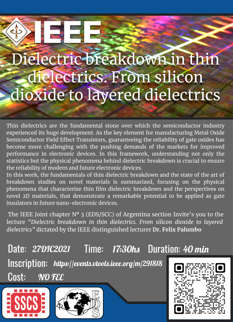
The IEEE Joint chapter Nº 3 (EDS/SCC) of Argentina section Invite´s you to the lecture “Dielectric breakdown in thin dielectrics. From silicon dioxide to layered dielectrics” dictated by the IEEE distinguished lecturer Dr. Felix Palumbo
Abstract
Thin dielectrics are the fundamental stone over which the semiconductor industry experienced its huge development. As the key element for manufacturing Metal Oxide Semiconductor Field Effect Transistors, guaranteeing the reliability of gate oxides has become more challenging with the pushing demands of the markets for improved performance in electronic devices. In this framework, understanding not only the statistics but the physical phenomena behind dielectric breakdown is crucial to ensure the reliability of modern and future electronic devices.
In this work, the fundamentals of thin dielectric breakdown and the state of the art of breakdown studies on novel materials is summarized, focusing on the physical phenomena that characterize thin film dielectric breakdown and the perspectives on novel 2D materials, that demonstrate a remarkable potential to be applied as gate insulators in future nano-electronic devices.
Date and Time
Location
Hosts
Registration
-
 Add Event to Calendar
Loading virtual attendance info...
Speakers
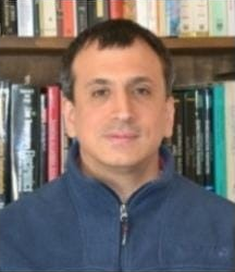
 Dr. Felix Palumbo
Biography:
Felix Palumbo has received the MSc. (2000) and the Ph.D. (2005) both in physics from the University of Buenos Aires, Argentina. He is an active researcher in the field of semiconductor device physics and reliability, with experience in the academy and industry.
From 2001 to 2002, he joined the R&D group of Tower Semiconductor at Migdal Haemek Israel, making research on reliability of gate oxides and flash memories. Since 2003 he was a repeat visiting scientist of different Institutions: the IMM-CNR Catania, Italy, the Universitat Autónoma de Barcelona, Spain, the Minatec Institute in Grenoble, France, and Soochow University, China.
From 2012 to 2014, he was visiting scientist at Technion Institute in Israel under a Marie Curie International Incoming Fellowship within the 7th European Community Framework Programme.
He managed several funded research projects in the field of radiation effects of CMOS technology and reliability of ultra-thin gates oxides, supported by CONICET, The Ministry of Science and Technology of the Argentinean Government and the Ministero degli Affari Esteri (MAE) of the Italian Government.At present, he is a research staff of the National Council of Science and Technology (CONICET), and a full professor at National Technological University (UTN) in Buenos Aires, Argentina. He is a reviewer of several scientific journals, author of four review articles, and of about 80 scientific and technical papers published in international peer-reviewed journals.
Address:Buenos Aires, Argentina

