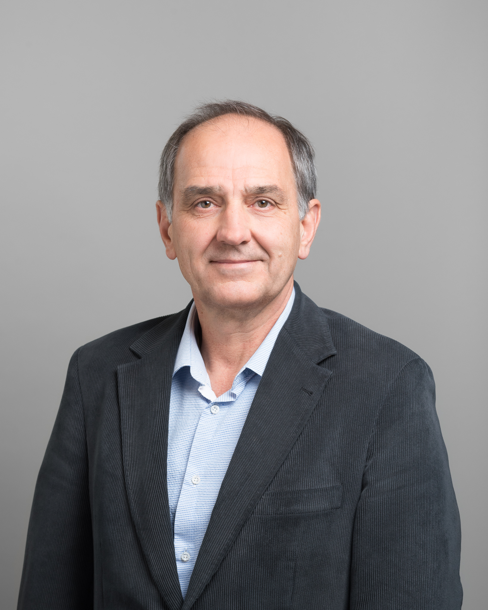
IEEE-EDS Seminar - Design and Modelling Challenges for Very Large-Scale Integrated Quantum Processors in Foundry CMOS Technologies by Sorin P. Voinigescu
Design and Modelling Challenges for Very Large-Scale Integrated Quantum Processors in Foundry CMOS Technologies by Sorin P. Voinigescu
This presentation will discuss the main challenges in the physical implementation, design, hierarchical modelling and simulation of the scalable qubit array and of the cryogenic control and readout electronics for future Quantum Processors with millions of qubits manufactured in commercial FDSOI and FinFET foundry technologies. Impact of process manufacturing rules restrictions and process variation on qubit design and modelling, circuit heat dissipation and layout miniaturization to fit the qubit array pitch, qubit-to-qubit crosstalk, and the need for atomistic, classical, and behavioural qubit simulation and modelling will be covered in detail.
Date and Time
Location
Hosts
Registration
-
 Add Event to Calendar
Loading virtual attendance info...
- Contact Event Host
- Co-sponsored by Circuits and Systems Society - CASS-SCV
Speakers
 Dr. Sorin P. Voinigescu of University of Toronto
IEEE-EDS Seminar - Design and Modelling Challenges for Very Large-Scale Integrated Quantum Processors in Foundry CMOS Te
Sorin P. Voinigescu is a Professor in the Electrical and Computer Engineering Department at the University of Toronto where he holds the Stanley Ho Chair in Microelectronics and is the Director of the VLSI Research Group. He is an IEEE Fellow and an expert on millimeter-wave and 100+Gb/s integrated circuits and atomic-scale semiconductor device technologies. He obtained his PhD degree in Electrical and Computer Engineering from the University of Toronto in 1994 and his M.Sc. Degree in Electronics and Telecommunications from the Politechnical Institute of Bucharest in 1984.
Biography:
Sorin P. Voinigescu is a Professor in the Electrical and Computer Engineering Department at the University of Toronto where he holds the Stanley Ho Chair in Microelectronics and is the Director of the VLSI Research Group. He is an IEEE Fellow and an expert on millimeter-wave and 100+Gb/s integrated circuits and atomic-scale semiconductor device technologies. He obtained his PhD degree in Electrical and Computer Engineering from the University of Toronto in 1994 and his M.Sc. Degree in Electronics and Telecommunications from the Politechnical Institute of Bucharest in 1984.
Agenda
This presentation will discuss the main challenges in the physical implementation, design, hierarchical modelling and simulation of the scalable qubit array and of the cryogenic control and readout electronics for future Quantum Processors with millions of qubits manufactured in commercial FDSOI and FinFET foundry technologies. Impact of process manufacturing rules restrictions and process variation on qubit design and modelling, circuit heat dissipation and layout miniaturization to fit the qubit array pitch, qubit-to-qubit crosstalk, and the need for atomistic, classical, and behavioural qubit simulation and modelling will be covered in detail.
Subscribe or Invite your friends to sign up for our mailing list and get to hear about exciting electron-device relevant talks. We promise no spam and try to minimize email. You can unsubscribe easily.
http://site.ieee.org/scv-eds/subscribe/

