Wide Bandgap Semiconductors: Opportunities and Challenges for Improved Modeling and Characterization Methods in Power Electronic Applications
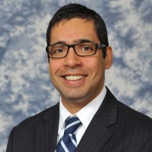
The combined Santa Clara Valley, San Francisco, & Oakland/East Bay IEEE PELS is very pleased to invite you to our first in-person event of 2023. We are excited and honored to have Prof. Raghav Khanna of the University of Toledo to speak on the topic of Wide Bandgap Semiconductors: Opportunities and Challenges for Improved Modeling and Characterization Methods in Power Electronic Applications
Wide bandgap semiconductor devices based on GaN and SiC offer myriads of advantages over traditional Si-based devices for applications in power electronics. These advantages include, among others, faster switching capabilities, allowing for reduced filtering components within converter topologies, thus leading to improved power density. Despite their many advantages, several challenges related to technological readiness level have hindered the widespread adoption of these devices. At the device-physics level, for example, the theoretical high voltage capability of GaN has yet to be commercially realized. At the device-circuits level, the fast-switching capability of SiC, though generally a beneficial attribute, has led to undesirable injected harmonic content into power electronic converters, leading to detrimental circuit-behavior. For these reasons, advanced modeling, and characterization methods for both GaN and SiC are needed, so that these devices can realize their full performance entitlement. This talk will present a broad array of modeling and characterization methodologies for GaN and SiC semiconductors. Device physics simulations using finite element modeling techniques will be presented, demonstrating the high voltage capability of vertical GaN diodes. It will be shown how these types of models can lead to the design and fabrication of future high voltage and reliable vertical GaN devices. Analytical physics-based models of GaN diodes, based on first principles, will also be presented. For these types of models, tradeoffs between model-fidelity and convergence-time in circuit-simulations will be discussed. Behavioral models of SiC MOSFETs, based on mathematical curve-fitted equations, will then be presented. These models will demonstrate the need to capture the frequency-dependence of the device’s parasitic per-terminal junction capacitances, as well as that of the parasitic package inductances, in order to construct a comprehensive empirically validated high-fidelity circuit-simulation. New strategies that can enable the development of hybrid-physics and -behavioral models will be presented, in a manner that offers utility to both device fabrication engineers, as well as application-circuit designers. For the various types of models presented, the importance of the interplay and refinement between simulation and empirical validation will be emphasized. This talk will conclude with characterization techniques and opportunities for wide bandgap semiconductors in space. The work presented in this talk lends itself well to developing strategies for multilevel integrated modeling infrastructures of next generation GaN and SiC devices, and to aid in the design, fabrication, and implementation of future high-voltage and reliable wide and ultrawide bandgap semiconductors.
Date and Time
Location
Hosts
Registration
-
 Add Event to Calendar
- 500 El Camino Real
- Santa Clara University’s Frugal Innovation Hub
- Santa Clara, California
- United States 95053
- Building: Sobrato Campus for Discovery and Innovation (SCDI)
- Room Number: 4th Floor, Room 4021
- Click here for Map
Speakers
 Prof. Raghav Khanna of The University of Toledo
WBG Semiconductors: Opportunities and Challenges for Improved Modeling and Characterization Methods in Power Electronics
Biography:
Raghav Khanna received the B.S. degree, M.S. degree, and Ph.D. degree in electrical engineering from the University of Pittsburgh, Pittsburgh, PA, USA in 2007, 2010, and 2014, respectively. Raghav has worked for several industries including Lockheed Martin (Philadelphia, PA), PPG Industries (Pittsburgh, PA) and HRL Laboratories (Malibu CA). At HRL, he was directly involved with the development of GaN based battery chargers for electric vehicles. In 2015, he joined the electrical engineering and computer science department at The University of Toledo. He is currently an Associate Professor and holds the position of Leidich Family Endowed Professor in Power and Energy Systems. His research interests are in characterization and modeling of wide bandgap semiconductors for applications in next generation power electronics, including; renewable energy, electric vehicles, aerospace and maritime systems, and in low power consumer electronics. He is also conducting extensive research on control strategies for integration of distributed energy resources. He recently received grants from the U.S. Department of Defense, U.S. Department of Energy, and NASA Jet Propulsion Laboratory to further develop his research activities.
Address:Toledo, Ohio, United States, 43606

