Heterogeneous Integration to enable AI Architectures
Abstract:
While silicon scaling has reached astonishing levels over the last half century, there has not been a corresponding level of scaling in electronic packaging technology. However, Artificial Intelligence (AI) architectures are now changing the landscape, increasingly moving us towards advanced packaging technology, especially Heterogeneous Integration (HI). What are these unique requirements of AI which are driving the need for HI? What are some of the unique challenges in semiconductor and packaging technologies that must be overcome to make this successful? This seminar will discuss key HI methods including interposers, fan out wafer level processing, silicon bridges, and 3D integration. We will look at their attributes as well as their challenges, to determine how they can be leveraged to achieve AI architectures.
Date and Time
Location
Hosts
Registration
-
 Add Event to Calendar
- Rochester Institute of Technology
- Rochester, New York
- United States 14623
- Building: Golisano Hall (Computing)
- Room Number: GOL-2400
- Click here for Map
Speakers
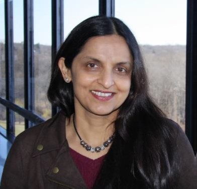
 Mukta Farooq of IBM Semiconductor Technology Research
Heterogeneous Integration to enable AI Architectures
Abstract:
While silicon scaling has reached astonishing levels over the last half century, there has not been a corresponding level of scaling in electronic packaging technology. However, Artificial Intelligence (AI) architectures are now changing the landscape, increasingly moving us towards advanced packaging technology, especially Heterogeneous Integration (HI). What are these unique requirements of AI which are driving the need for HI? What are some of the unique challenges in semiconductor and packaging technologies that must be overcome to make this successful? This seminar will discuss key HI methods including interposers, fan out wafer level processing, silicon bridges, and 3D integration. We will look at their attributes as well as their challenges, to determine how they can be leveraged to achieve AI architectures.
Biography:
Mukta G. Farooq, PhD
Distinguished Research Staff Member, Master Inventor IBM Semiconductor Technology Research
IEEE Fellow, EDS Distinguished Lecturer
Dr. Mukta Farooq is an IBM Distinguished Research Staff Member, and the 3D/Heterogeneous Integration Technology Leader for the AI Hardware Center at IBM Research. She is an IEEE Fellow, an IEEE EDS Distinguished Lecturer, and a Distinguished Alumna of IIT-Bombay (India). Mukta is a metallurgist and materials scientist with expertise in Heterogeneous and 3D Integration for Chiplet Technology, CMOS BEOL, Lead-free Alloys, and Chip Package Interaction. She has 231 granted US patents, 66 granted international patents, and is an IBM Lifetime Master Inventor and IBM Academy of Technology member. She has been invited to give keynote talks and teach short courses at top conferences, and to write papers in her field of expertise. Mukta received her BS from IIT-Bombay, MS from Northwestern University, and PhD from Rensselaer Polytechnic Institute.
Agenda
12:00 noon: pizza is served
12:15PM: talk begins
1PM: Q&A, discussion, refreshments

