New group IV materials and challenges for applications convergence in Si -CMOS Technology
IEEE EDS - Seventh Mexico Technical Meeting 2023 (MTM_7-2023)
Mexico Chapter and CINVESTAV-IPN Student Branch Chapter
Center for Research and Advanced Studies of the National Polytechnic Institute
On the behalf of the Seventh IEEE-EDS Mexico Technical Meeting 2023 (MTM_7-2023), organized jointly by the IEEE EDS CINVESTAV-IPN Student Branch Chapter from the Section of Solid-State Electronics at the Center for Research and Advanced Studies of the Polytechnic National Institute (CINVESTAV-IPN), we extend the invitation for the conference with an Peter Grüberg Institute 9.
The MTM_7-2023 will be held SEES bunker room at June 30th, 2023.
Date and Time
Location
Hosts
Registration
-
 Add Event to Calendar
- Av Instituto Politécnico Nacional 2508, San Pedro Zacatenco, Gustavo A. Madero, 07360 Ciudad de México, CDMX
- Sección de Electrónica del Estado Solido
- Cd. De México, Mexico
- Mexico 07360
- Building: Sección de Electrónica del Estado Solido Aula: bunker
- Contact Event Hosts
-
M.C. Luz Balcazar; iq.maggy_@hotmail.com Tel. 57473800 Ext. 6265
Ing. Abril Garcia; abril.garcia.soriano@cinvestav.mx Tel. 57473800 Ext. 6265
- Co-sponsored by Center for Research and Advanced Studies of the National Polytechnique Institute, CINVESTAV-IPN.
- Starts 29 June 2023 01:00 AM UTC
- Ends 30 June 2023 09:00 PM UTC
- No Admission Charge
Speakers
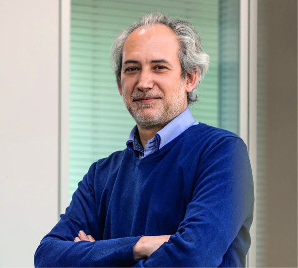 Prof. Dan of Peter Grünberg Institute
New group IV materials and challenges for applications convergence in Si -CMOS Technology
The activity focus is placed on the development of GeSn and SiGeSn epitaxy for photonics, electronics and energy harvesting applications. We were the first group worldwide able to experimentally demonstrate that the GeSn alloys become fundamental direct bandgap semiconductors. The evident consequence was the proof of laser emission in GeSn on Si substrates. Advanced epitaxy developed in the group allows the demonstration first and still unique lasers like Multi quantum Wells laser, cw laser operation at low temperatures or vertical NWs GeSn/Ge nano-MOSFETs. Presently the group was able to show room temperature tensely strained GeSn lasers, electrically pumped GeSn lasers, GeSn based CMOS invertor and low thermal lattice conductivity as required for energy harvesting.
The long standing cooperation with the CEA-LETI and the epitaxy group in LETI has contributed to the development of the GeSn field and led to multiple publications and project cooperation’s.
Email:
Address:Wilhelm-Johnen-Straße, 52428 Jülich, Alemania, , Jülich, Germany
Agenda
Schedule Tuesday 30th—SEES Bunker room Speaker
11:00 - 11:10 Presentation of Dr. Dan Buca Dr. Arturo Escobosa
11:10 - 13:00 New group IV materials and challenges for Dr. Dan Buca
applications convergence in Si -CMOS Technology
MTM_7-2023 is an IEEE-EDS sponsored technichal meeting. Co-sponsored by the Section of Solid-Sate Electronics at the Center for Research and Advanced Studies of the National Polytechnic Institute.