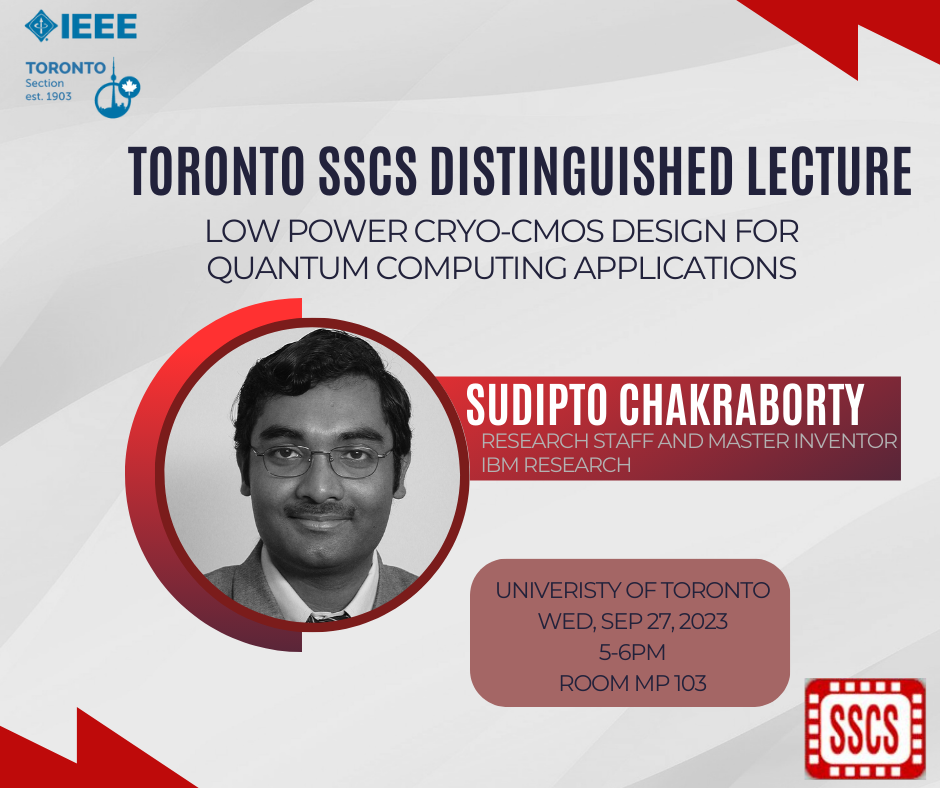
Low power cryo-CMOS design for quantum computing applications

This talk will cover practical challenges for cryogenic CMOS designs for next generation quantum computing. Starting from system level, it will detail the design considerations for a non-multiplexed, semi-autonomous, transmon qubit state controller (QSC) implemented in 14nm CMOS FinFET technology. The QSC includes an augmented general-purpose digital processor that supports waveform generation and phase rotation operations combined with a low power current-mode single sideband upconversion I/Q mixer-based RF arbitrary waveform generator (AWG). Implemented in 14nm CMOS FinFET technology, the QSC generates control signals in its target 4.5GHz to 5.5 GHz frequency range, achieving an SFDR > 50dB for a signal bandwidth of 500MHz. With the controller operating in the 4K stage of a cryostat and connected to a transmon qubit in the cryostat’s millikelvin stage, measured transmon T1 and T2 coherence times were 75.7μs and 73μs, respectively, in each case comparable to results achieved using conventional room temperature controls. In further tests with transmons, a qubit-limited error rate of 7.76x10⁻⁴ per Clifford gate is achieved, again comparable to results achieved using room temperature controls. The QSC’s maximum RF output power is -18 dBm, and power dissipation per qubit under active control is 23mW.
Date and Time
Location
Hosts
Registration
-
 Add Event to Calendar
- University of Toronto
- 255 Huron Street
- Toronto, Ontario
- Canada M5S 1A7
- Building: McLennan Physical Laboratories
- Room Number: MP 103
- Click here for Map
Speakers
Sudipto Chakraborty of IBM Research
Low power cryo-CMOS design for quantum computing applications
Biography:
Sudipto Chakraborty received his B. Tech from Indian Institute of Technology, Kharagpur in 1998 and Ph.D in EE from Georgia Institute of Technology in 2002. He worked as a researcher in Georgia Electronic Design Center (GEDC) till 2004. From 2004 to 2016, he was a senior member of technical staff at Texas Instruments where he contributed to low power integrated circuit design in more than 10 product families in the areas of automotive, wireless, medical and microcontrollers. Since 2017, he has been working at the IBM T. J. Watson Research Center where he leads the low power circuit design for next generation quantum computing applications using nano CMOS technology nodes. He has authored or co-authored more than 75 papers, two books and holds 87 US patents. He has served in the technical program committees of various conferences including CICC, RFIC, IMS and has been elected as an IBM master inventor in 2022 for his contributions.

