Communications between Chiplets – Bridge
Chiplet is a chip design method and heterogeneous integration is a chip packaging method. Chiplet design and heterogeneous integration packaging have been generated lots of tractions lately. For the next few years, we will see more implementations of a higher level of chiplet designs and heterogeneous integration packaging, whether it is for cost, time-to-market, performance, form factor, or power consumption. In this lecture, the following topics will be covered: (1) System-on-Chip (SoC); (2) Why Chiplet Design; (3) Chiplet Design and Heterogeneous Integration Packaging (a) Chip Partition and Chip Split, (b) Chip partition and Heterogeneous Integration, (c) Chip split and Heterogeneous Integration, and (d) Advantages and Disadvantages; (4) Lateral Communication between Chiplets (e.g., Bridges) (a) Bridge Embedded in Build-up Package Substrate, (b) Bridge Embedded in Fan-Out EMC with RDLs, (c) UCIe, and (d) Hybrid Bonding Bridge; (5) Chiplet Design and Heterogeneous Integration Packaging (a) Multiple System and Heterogeneous Integration with Package Substrate (2D IC Integration), (b) Multiple System and Heterogeneous Integration with Thin Film layer on the Package Substrate (2.1D IC Integration), (c) Multiple System and Heterogeneous Integration with TSV-less (Organic) Interposer (2.3D IC Integration), (d) Multiple System and Heterogeneous Integration with Passive TSV-Interposer (2.5D IC Integration) for artificial intelligence applications, and (e) Multiple System and Heterogeneous Integration with Active TSV-Interposer (3D IC Integration); (6) Summary; (7) Trends in Chiplet Design and Heterogeneous Integration Packaging.
Date and Time
Location
Hosts
Registration
-
 Add Event to Calendar
- 6455 Lusk Blvd
- (Building entry details to be sent on March 12th)
- San Diego, California
- United States 92121
- Building: Qualcomm Building Q
Speakers
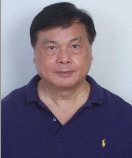
 John Lau of Unimicron Technology Corporation
Communications between Chiplets – Bridge
Chiplet is a chip design method and heterogeneous integration is a chip packaging method. Chiplet design and heterogeneous integration packaging have been generated lots of tractions lately. For the next few years, we will see more implementations of a higher level of chiplet designs and heterogeneous integration packaging, whether it is for cost, time-to-market, performance, form factor, or power consumption. In this lecture, the following topics will be covered: (1) System-on-Chip (SoC); (2) Why Chiplet Design; (3) Chiplet Design and Heterogeneous Integration Packaging (a) Chip Partition and Chip Split, (b) Chip partition and Heterogeneous Integration, (c) Chip split and Heterogeneous Integration, and (d) Advantages and Disadvantages; (4) Lateral Communication between Chiplets (e.g., Bridges) (a) Bridge Embedded in Build-up Package Substrate, (b) Bridge Embedded in Fan-Out EMC with RDLs, (c) UCIe, and (d) Hybrid Bonding Bridge; (5) Chiplet Design and Heterogeneous Integration Packaging (a) Multiple System and Heterogeneous Integration with Package Substrate (2D IC Integration), (b) Multiple System and Heterogeneous Integration with Thin Film layer on the Package Substrate (2.1D IC Integration), (c) Multiple System and Heterogeneous Integration with TSV-less (Organic) Interposer (2.3D IC Integration), (d) Multiple System and Heterogeneous Integration with Passive TSV-Interposer (2.5D IC Integration) for artificial intelligence applications, and (e) Multiple System and Heterogeneous Integration with Active TSV-Interposer (3D IC Integration); (6) Summary; (7) Trends in Chiplet Design and Heterogeneous Integration Packaging.
Biography:
John H Lau, with more than 40 years of R&D and manufacturing experience in semiconductor packaging, has published more than 515 peer-reviewed papers (375 are the principal investigator), 40 issued and pending US patents (25 are the principal inventor), and 23 textbooks (all are the first author), e.g., Chiplet Design and Heterogeneous Integration Packaging (Springer, 2023). John is an elected IEEE fellow, IMAPS Fellow, and ASME Fellow and has been actively participating in industry/academy/society meetings/conferences to contribute, learn, and share.

