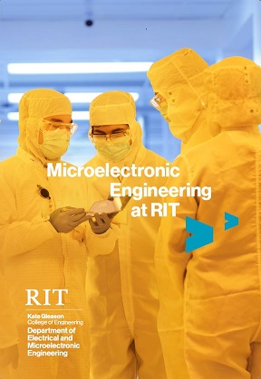
42nd Annual Microelectronic Engineering Conference at RIT
This conference brings together students, faculty, alumni, friends and industry guests interested in Microelectronic Engineering. Key elements of the conference are: technical presentations by seniors on their capstone research and design projects, industry and alumni presentations, recognition of companies who have supported the program, review of program activities and achievements over the past year and industry feedback on student and academic program activities.
The event begins on Monday evening with a reception and dinner at the RIT Inn & Conference Center. The reception starts at 5:30pm, with dinner at 6:30pm and speakers to follow.
Off-campus map - RIT Inn & Conference Center
The technical session is on Tuesday from 8am - 4pm in the Center for Integrated Manufacturing (CIMS, SLA/078).
Campus map - CIMS Conference Center
Registration is required (no charge) to determine meal orders.
Date and Time
Location
Hosts
Registration
-
 Add Event to Calendar
- Rochester Institute of Technology
- One Lomb Memorial Drive
- Rochester, New York
- United States 14623
- Building: CIMS / Slaughter Hall SLA/078 (campus map)
- Room Number: 2210 - 2240
- Click here for Map
- Contact Event Host
-
Karl Hirschman (click above)
Robert Pearson, repemc@rit.edu (email)
- Starts 30 March 2024 04:00 AM UTC
- Ends 19 April 2024 04:00 AM UTC
- No Admission Charge
Speakers
Baljit Singh of Ajuba
Semiconductor Synergy: India's Semiconductor Landscape and Collaborations with RIT
Biography:

Baljit Singh, CEO of Ajuba has been involved in providing strategy, business development and sales & marketing services to manufacturers and service providers seeking to operate in India, Israel and USA. Baljit has a degree in microelectronic engineering from Rochester Institute of Technology, in 1993. Baljit has been fortunate to be part of teams that have brought innovation and game changer products & services to the market. Baljit worked as a Process Engineer at Xerox Corporation where the team developed Thermal Inkjet Chips. Today the world of printers has shrunk with the innovation of Thermal Inkjet Chip. He then joined Analog Devices as a Process Engineer and was part of the team that brought the Accelerometer Chip, the chip that controls Airbags in cars. With ADE Corporation in Boston, as a Product Manger he led the effort to bring the world’s first automated fuzzy logic defect classification system for the semiconductor industry. From ADE he joined Opal Technologies to bring the world’s fully automated Scanning Electron Microscope (SEM) to the market. Opal Technologies got acquired by Applied Materials and he then started his first services company in 1998 which reached a revenue of over one million USD in less than a year. He then embarked into a products start-up company where in less than a year all the major semiconductor companies world-wide were using their Data Analysis products. With Ajuba, he is currently driving cross border partnership between India-Israel-North America.
Todd Layer of Wolfspeed
Wolfspeed Powering and Manufacturing the Possibilities
Biography:
Todd Layer, MicroE BS ‘87, Director, Equipment and Maintenance Engineering North Carolina Fabs (NCF), Wolfspeed
Ben Eynon of Lam Research
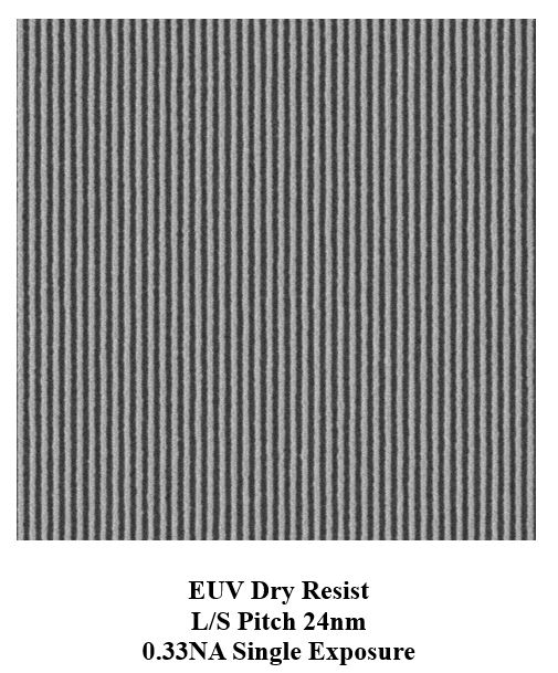
EUV Dry Resist and Process for 2nm Node Patterning and Beyond
Extreme ultraviolet (EUV) lithography has been introduced into semiconductor IC high volume manufacturing (HVM) beginning at the 7nm node logic, and is being qualified for an increasing proportion of litho steps at 5/3nm Logic and 16/14nm DRAM. A persistent challenge for the EUV scanner is to supply to the photoresist (PR) a high contrast image with enough photons to meet HVM productivity targets with acceptable dimensional and defectivity control. Local stochastic variability in dimension and placement dominates the total dimension control budget, and reducing that variability by increasing the exposure dose comes at the cost of scanner throughput.
EUV scanner power and reliability have each made significant improvements toward performing at the HVM level over the last 10 years; however photoresists have not kept pace with the increasingly stringent technology requirements. Today spin-on photoresists are unable to meet the sensitivity, resolution, edge roughness, and defectivity targets for the high volume manufacturing (HVM) of the most advanced technology nodes. This gap in photoresist readiness has driven customers to make compromises in design and cost and put significant pressure on downstream processes to correct for shortcomings in the lithography pattern, providing a significant opportunity for breakthrough innovation.
We discuss here our revolutionary technique to both apply EUV photoresist and develop latent images in the photoresist using dry technologies instead of the existing wet spin coating and development that have been in use over the last several decades. We will review the key mechanisms and advantages of dry resist processing over wet resist processing, and will report the latest results across a variety of key indices. This nascent technology has demonstrated best-in-class resist performance at leading edge design rules and now opens the door to a new level of performance in EUV lithography patterning.
Biography:

Ben Eynon, MicroE BS ’87, Lam Research
After graduating from RIT’s Microelectronic Engineering program in 1987, Benjamin Eynon has spent the majority of his 35+year career in the semiconductor industry in engineering, management, and executive roles in the areas of R&D, high volume manufacturing, marketing, and new business development. In 2005, he published a book entitled “Photomask Fabrication Technology” which has served as the handbook for the industry ever since. He has four patents and has published over 40 technical articles. As a SEMATECH assignee from Samsung’s Advanced Lithography Division, he led the EUV Resist Test Center and the EUV Mask Blank Development center as SEMATECH’s Associate Director of Lithography. Afterward at Samsung Austin Semiconductor in Texas, he led the facility’s Lithography Division and then led the development and installation of the world’s first and largest 14nm FinFET semiconductor wafer manufacturing process. He is now working at Lam Research heading up ATD Marketing, bringing dry resist processing and infrastructure to the EUV lithography ecosystem.
Mycahya Eggleston of Micron Technology
Critical Dimension Uniformity - Every Angstrom Counts
As technology nodes shrink, budgets for patterning variation also shrink. Properly quantifying these process or patterning variations and identifying the sources of variation is becoming more and more critical to ensure devices will have a path to become a yielding part in high volume manufacturing. Critical Dimension Uniformity (CDU) metrics complement overlay metrics to form a more complete estimation of total process and patterning variation. CDU variation must be broken down into both systematic and random components, with assignments for lot-level, wafer-level, within-wafer, within-field, within-die, and within feature level variation sources. Understanding which systematic, and which random variation sources can be controlled or minimized and by how much is a fundamental part of CDU methodology. This work is a combination of statistical, modeling, and empirical study, coupled with deep process knowledge.
This presentation will highlight some of the methodology used by the CDU team in collaboration with process development, data science, and modeling teams as they work to understand the variation and implement changes to minimize the total variation in the process, while also ensuring that the device can meet fundamental electrical device characteristics for operation.
Biography:
Mycahya Eggleston, Senior Engineer, Critical Dimension Uniformity, Micron Technology
Mycahya Eggleston graduated from MCC with an AAS degree in Electrical Engineering in 2014 and RIT with a BS degree in Micro-electronic Engineering in 2017. He joined Micron Technology after graduation on the technology development Photo shift team. In 2019 he became the first team member of the newly formed CD Uniformity group. He currently serves as a Senior CDU Applications Engineer and has developed and integrated multiple methodologies for quantifying Critical Dimension Uniformity (CDU) on the past three DRAM technology nodes, including methods for budgeting variation across multiple length scales and defining the maximum variation possible for device operation.
Lynn Fuller of Rochester Institute of Technology
The Importance of Actually Teaching CMOS Manufacturing In a University Lab Setting
Biography:
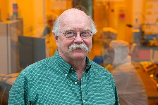
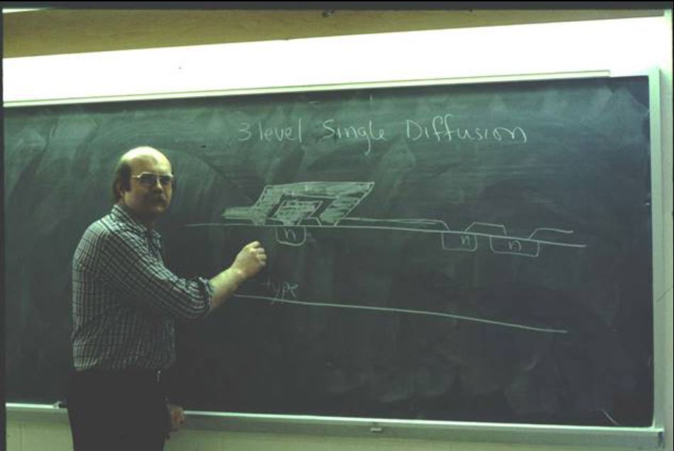
Dr. Lynn Fuller, BSEE ’69, RIT Microelectronic Engineering program founder, EME Professor Emeritus
Agenda
Monday April 22, 2024
5:30 p.m. Reception at the RIT Inn and Conference Center
Dinner Agenda
6:30 p.m. Dinner Begins
7:00 p.m. Program Begins
Welcome by Dr. Karl Hirschman, Micron Professor, Microelectronic Engineering Program Director
“Semiconductor Synergy: India's Semiconductor Landscape and Collaborations with RIT”, Baljit Singh, BS MicroE ‘93, CEO of Ajuba USA/India.
“Microelectronic Engineering – The Year in Review”, Dr. Robert Pearson, Past Director of the Microelectronic Engineering Program
Awards
- Dr. Renan Turkman Scholarship Award Announcement
- Dr. Lynn Fuller Scholarship Award Announcement
Closing Remarks: Dr. Karl Hirschman
Tuesday April 23, 2024
8:00 – 8:30 a.m. Registration CIMS
Technical Program Agenda
Morning Session AM-1
Session Chair: Dr. Robert Pearson, Associate Professor
8:30 a.m. Opening Remarks, Dr. Karl Hirschman, Micron Professor, Microelectronic Engineering Program Director
8:35 a.m. “Wolfpeed Powering and Manufacturing the Possibilities“, Todd Layer, MicroE BS ‘87, Director, Equipment and Maintenance Engineering, North Carolina Fabs (NCF), Wolfspeed
9:05 a.m. “Micro Transfer Printing Tool Characterization”, Trevor Woodard, Senior MicroE ‘24
9:25 a.m. “Fabrication of a Metal-Dielectric DUV Band-pass Optical Filter”, Ian Endres, Senior MicroE ‘24
9:45 a.m. BREAK and Posters
Morning Session AM-2
Session Chair: Dr. Karl Hirschman, Micron Professor
10:15 a.m. “EUV Dry Resist and Process for 2nm Node Patterning and Beyond”, Ben Eynon, MicroE BS ’87, Lam Research
10:45 am “An Exploration of SiC Top-Down Microfabrication Methods”, Laura Armellino, Senior MicroE ‘24
11:05 a.m. " Germanium Detectors for the Infrared Spectrum”, Ceili Lipp, Senior MicroE ‘24 24
11:25 a.m. “Analysis of performance of IGZO TFTs”, Alex Moore, Senior MicroE ‘24
11:45 a.m. LUNCH
Afternoon Session PM-1
Session Chair: Sean Rommel, Professor
1:00 p.m. Upwards Remarks, Parsian Mohseni, Associate Professor
1:05 p.m. “Critical Dimension Uniformity - Every Angstrom Counts”, Mycahya Eggleston, BS MicroE ’17, Senior Engineer, Critical Dimension Uniformity, Micron Technology
1:35 p.m. “Cleanroom MES and SPC Systems Design and Implementation”, Carl Kulesza, Senior MicroE ‘24
1:55 p.m. “Radiation Hardening of a III-V Solar Cell Via Graded Doping”, Katelynn Blank, Senior MicroE ‘24
2:15 p.m. BREAK
Afternoon Session PM-2
Session Chair: Michael Jackson, Associate Professor
2:30 p.m. “The Importance of Actually Teaching CMOS Manufacturing in a University Lab Setting”, Dr. Lynn Fuller, RIT Professor Emeritus
3:00 p.m. “Development of a Dry Etching Process for Germanium”, Dylan Bruno, Senior MicroE ‘24
3:20 p.m. “Thin Film Optical Filter for Astronomical Applications”, Tucker Dunham, Senior MicroE ’24
3:40 p.m. Technical Session Closing Remarks - Dr. Sean Rommel