Advanced Substrates for Chiplets and Heterogeneous Integration
Advanced Substrates for Chiplets and Heterogeneous Integration
John H Lau, Unimicron Technology Corporation
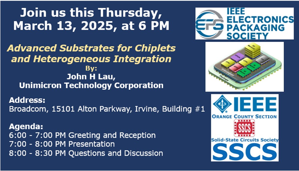
Today, most of the package substrates for HPC driven by AI (artificial intelligence) are made by the 2.5D IC integration. In general, for 2.5D or CoWoS (chip on wafer on substrate), the SoC and high bandwidth memories (HBMs) are supported by a TSV-interposer and then solder bump and underfill on a build-up package substrate. However, because of the ever-increasing size of the TSV-interposer, the manufacture yield loss of the TSV-interposer is becoming unbearable. The key players such as NVIDIA, AMD, Intel, SK Hynix, Samsung, Micron, TSMC, etc. are working very hard to eliminate the TSV interposer and put the HBMs directly on top of the SoC (3.3D IC integration). Front-end integration of some of the chiplets (before package heterogeneous integration) can yield a smaller package size and a better performance (3.5D IC integration). In the past few years, 2.3D IC integration or CoWoS-R is getting lots of traction. The motivation is to replace the TSV-interposer with a fan out fine metal L/S redistribution-layer (RDL)-substrate (or organic-interposer). In general, for 2.3D, the package substrate structure (hybrid substrate) consists of a build-up package substrate, solder joints with underfill, and the organic-interposer. Today, 2.3D is already in production. During IEEE/ECTC 2023, TSMC published two papers on replacing the large-size TSV-interposer by LSIs (local silicon interconnects, i.e. Si bridges) and embedding the LSIs in fan-out RDL-substrate. TSMC called it CoWoS-L. Recently, since Intel’s announcement (September 18, 2023) on the glass core substrate for their one-trillion transistors to be shipped before 2030, glass core substrate has been a very hot topic. Since the shipments of co-packaged optics (CPO) by Intel and Broadcom CPO has been getting lots of tractions. In this lecture, the introduction, recent advances, and trends in the substrates of 3.5D IC integration, 3.3D IC integration, 3D IC integration, 2.5D IC integration, 2.3D IC integration, 2.1D IC integration, 2D IC integration, fan-out RDL, embedded Si-bridge, CoWoS-R, CoWoS-L, CPO, and glass core for HPC driven by AI will be discussed. Some recommendations will be provided.
Date and Time
Location
Hosts
Registration
-
 Add Event to Calendar
- 15101 Alton Parkway
- Irvine, California
- United States 92618
- Building: Building #1
- Starts 26 February 2025 03:00 AM UTC
- Ends 13 March 2025 07:00 AM UTC
- No Admission Charge
Speakers
John Lau
Advanced Substrates for Chiplets and Heterogeneous Integration
Biography:
John H Lau, with more than 40 years of R&D and manufacturing experience in semiconductor packaging, has published more than 535 peer-reviewed papers (385 are the principal investigator), 52 issued and pending US patents (31 are the principal inventor), and 23 textbooks (all are the first author). John is an elected IEEE fellow, IMAPS Fellow, and ASME Fellow and has been actively participating in industry/academy/society meetings/conferences to contribute, learn, and share.
Email:
Agenda
6:00-7:00PM Greeting and reception
7:00-8:00PM Advanced Substrates for Chiplets and Heterogeneous Integration presentation by John Lau
8:00-8:30PM Questions and Discussion
Media
| IEEE_SSCS_Event_on_March_13_2025_-_Farhad_Mafie | 139.08 KiB |