IEEE EPS RPI / EDS MHV - 2nd Mini-Colloquium: Semiconductor Technology Evolution
The IEEE EDS/EPS MHV and RPI Chapters are excited to announce the upcoming 2nd Mini-Colloquium (MQ) 2025 on Semiconductor Technology Evolution, which will take place at CBIS Auditorium, RPI campus, on April 18th, 2025.
This occasion presents a unique chance to gain insights from industry experts, delve into topical issues, and explore potential career opportunities as part of the CHIPS Workforce Development initiative.
The event is open to ALL! No IEEE membership required to register. Registration is mandatory to attend.
Date and Time
Location
Hosts
Registration
-
 Add Event to Calendar
- 110 8th St
- Troy, New York
- United States 12180
- Building: Center for Biotechnology and Interdisciplinary Studies
- Room Number: Auditorium and Gallery
- Contact Event Hosts
- Co-sponsored by EDS MHV Chapter
- Starts 20 March 2025 04:00 AM UTC
- Ends 18 April 2025 04:00 AM UTC
- No Admission Charge
Speakers
Dr. Poliks of Binghamton University, State University of New York
Enabling Hybrid and Additive Approaches To Medical and Industrial Devices
The concepts and advancement of printed wiring boards and chip packaging are well established. But “wearable” applications continue to drive the need to dramatically reduce the size, weight, and power requirements leading to minimizing in both the thickness of the substrate and the silicon devices.
Flexible and hybrid electronics (FHE) combine additively printed electronics on bendable, flexible or highly stretchable substrates with the performance of thinned silicon-based semiconductors to enable applications that include wearable medical devices and industrial sensors. Many of these applications require thin, soft, conformal, or stretchable attributes for "wearability" in human healthcare or integration on industrial or infrastructure systems that must survive extreme conditions. Some applications require the electronics to be printed “in-place” on existing surfaces and components.
This presentation will review the design and fabrication challenges associated with interfacing hard and soft electronic components, the use of sustainable materials and particle-free inks, printing and processing methods, and testing of FHE systems. Enabling features that include the use of highly stretchable conductors, fluid transport, printed electrochemical sensors, RF devices, power conversion, and efforts to enable use at extreme conditions that include high temperature, power and current operation will be described. System “concepts of operation” will guide the evaluation of performance and reliability. Outcomes from this work are expected to inform the eventual scale-up to large area, roll-to-roll manufacturing or integration on complex, non-planar surfaces and solids.
Biography:
Mark D. Poliks is a SUNY Distinguished Professor and Empire Innovation Professor of Materials Science and Engineering and Systems Science and Industrial Engineering at the Thomas J. Watson College of Engineering and Applied Science, Binghamton University, State University of New York. He is the founding director of the Center for Advanced Microelectronics Manufacturing (CAMM), a New York State Center of Advanced Technology and home to the New York Node of the federally supported NextFlex Manufacturing USA. Poliks has made sustained contributions to the fields of materials processing, electronics packaging, flexible, hybrid and additive electronics that are relevant to a variety of medical and industrial applications.
Poliks was the General Chair of the 69th IEEE Electronic Components and Technology Conference (ECTC). He was a recipient of the 2017 SUNY Chancellor's Award for Excellence in Research, is a Fellow of NextFlex, an elected member of the IEEE Electronics Packaging Society (EPS) Board of Governors and serves as the director of student programs and is an IEEE Distinguished Lecturer.
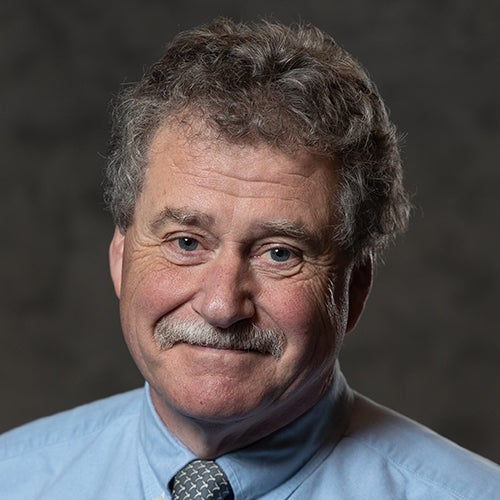
Dr. Lau of Unimicron Technology Corporation
Flip Chip Technology – Solder Bumps, Microbumps, and Bumpless Cu-Cu Hybrid Bonding
Since IBM's invention of flip chip tech in the 1960s, major strides have been made—from C4 bumps to C2 (Cu-pillar bumps), fan-out RDLs, and now bumpless Cu-Cu hybrid bonding. This talk highlights the evolution, current trends, and recommendations.
Outline:
- Introduction
- Wafer Bumping: The Mother of Flip Chip
- Substrate Technologies:
- Organic
- Silicon
- Glass
- Fan-out RDLs - Flip Chip Assembly:
- Mass Reflow (C4/C2, CUF)
- TCB Low-Force + Reflow (C4/C2, CUF)
- TCB High-Force (C2, NCP)
- TCB High-Force (C2, NCF)
- Cu-Cu Hybrid Bonding - Reliability:
- Post-Assembly Underfill
- Pre-Assembly Underfill - Summary & Recommendations
Biography:
John H Lau, with more than 40 years of R&D and manufacturing experience in semiconductor packaging, has published more than 530 peer-reviewed papers (385 are the principal investigator), 52 issued and pending US patents (31 are the principal inventor), and 24 textbooks. John is an elected IEEE fellow, IMAPS Fellow, and ASME Fellow and has been actively participating in industry/academy/society meetings/conferences to contribute, learn, and share.
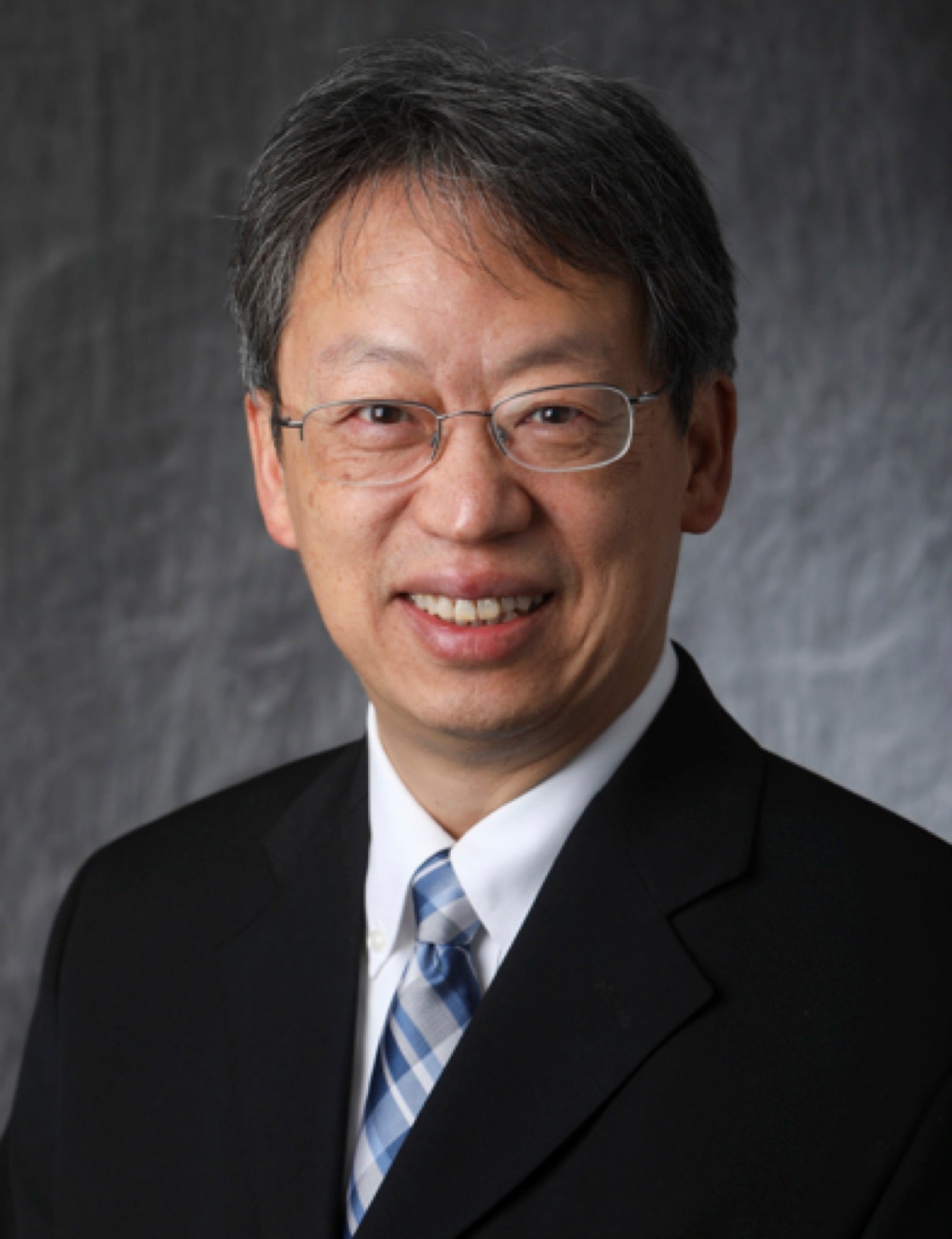
Dr. Joshi of IBM
Invaluable Memories
The enormous global growth in AI, Generative AI, and LLM has pushed GPU and CPU performance, memory capacity, bandwidth, and power to their limits. Memory bandwidth and performance continue to be bottlenecks for these applications. Technology scaling slow down does not help to resolve this bottleneck. However, innovations in this field will continue and may open new ways for future computation. Additional push for System and Design Technology co-optimization (STCO) and (DTCO), respectively.is rejuvenating chip fabrication development. An additional push beyond technology scaling for chiplets, photonics in packaging, and Universal Component Interface (UCI) standardization, HBM-like memory is helping in memory capacity and bandwidth areas. Compute In Memory (CIM) is another example of memory utilization for increasing performance. Thus, memories are the workhorses of the semiconductor industry as they are key and integral parts of CPUs and GPUs and occupy 50%-60% of the area of processors. Volatile and non-volatile memories (NVM) have proved to be focal points for research over decades. Applications of these spread across many domains such as Artificial Intelligence (AI), servers, high-performance computing, Systems on Chip (SOC), Internet of Things (IoT), quantum computing, etc., and thus are essential components of the computing world. This talk covers such memories and showcases their impact from the IBM and rest of the industry perspective. As we march forward, the scaling of memories poses a major challenge to achieving functionality, performance, area, power, and yield. To overcome scaling issues, the talk will describe alternative techniques and circuits and bring out future challenges.
Biography:
Dr. Rajiv V. Joshi is an IEEE Life Fellow, winner of the prestigious IEEE Daniel Noble award, IEEE Circuit and System Society Vice President of Industry, and a key technical lead/Research Scientist at T. J. Watson Research Center, IBM. He received his B. Tech IIT (Bombay, India), M.S (MIT), and Dr. Eng. Sc. (Columbia University). He has successfully led innovations in technology, memories (SRAM, DRAM, and others), and predictive analytic techniques for yield prediction for IBM Server Groups and their products. His statistical techniques are tailored for machine learning and AI, which are licensed and commercialized. His memory innovations and work are used in both IBM P and Z servers. His technology innovations set IBM’s leadership across the globe. He received 3 Outstanding Technical Achievement (OTAs), 3 highest Corporate Patent Portfolio awards for contributions in interconnect technologies, holds 73 invention plateaus, has over 290 US patents covering front end and back end of the line processes, and structures, volatile and non-volatile memories, Compute in Memory structures, machine learning algorithms, and quantum computing and over 425 international patents. He has authored and co-authored over 235 refereed papers, delivered over 60 invited/keynote talks, and given several Seminars. He received the NY IP Law Association's Inventor of the Year award in Feb. 2020. He is a Mercator Fellow at the University of Siegen, Germany. He received an industrial pioneer award in 2014 from the IEEE Circuits and Systems Society. He received the Best Editor Award from the IEEE TVLSI journal. He was inducted into the New Jersey Inventor Hall of Fame in Aug 2014. He won the Mehboob Khan Award two times from Semiconductor Research Corporation. He won several best paper awards from ISSCC 1992, VMIC 1998, ICCAD 2009, and ISQED 2014. He is a member of the IBM Academy of Technology and a master inventor. He serves on the Board of Governors for IEEE CAS as an industrial liaison. He served on EC for DAC, ISLPED, CICC, ISCAS, AICAS, and APCCAS (2023) committees, as well as the AE of TCAS I and TVLSI. He served as a Distinguished Lecturer for IEEE CAS, CEDA, and EDS society. He is an ISQED and World Technology Network fellow and a distinguished alumnus of IIT Bombay. He served on the executive advisory committee for the Center of 3D Ferroelectric and Microelectronics at Penn State. He serves as an IEEE CAS Ambassador to India.

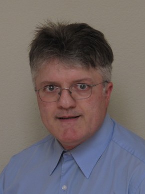
Dr. Kerber of Intel
Reliability of Metal Gate / High-K CMOS devices
Aggressively scaled transistor technologies with metal gate/high-k stacks encounter additional reliability challenges beside bias temperature instability (BTI) in PMOS and NMOS devices, time dependent dielectric breakdown and hot carrier degradation. Time-zero variability and variability induced by device aging is a growing concern which needs to be modeled using stochastic processes. The physical nature of the stochastic process remains under debate and to support model development efforts large statistical data sets are essential. In addition, self-heating during reliability testing can be observed in novel device structures like bulk FinFET, SOI FinFETs, FDSOI and gate-all-around devices and needs proper attention. Furthermore, to increase the confidence in the discrete device reliability models, device-to-circuit correlations need to be established. In this presentation we discuss how to obtain stochastic BTI data for discrete SRAM and logic device beyond 3s, address device-to-circuit correlations using ring-oscillators and explore self-heating effects in FinFET and SOI devices.
Biography:
Andreas Kerber received his Diploma in physics from the University of Innsbruck, Austria, in 2001, and a PhD in electrical engineering from the TU-Darmstadt, Germany, with honors in 2004. From 1999 to 2000 he was an intern at Bell Laboratories, Lucent Technologies (Murray Hill, NJ, USA) working on the electrical characterization of ultra-thin gate oxides. From 2001 to 2003, he was the Infineon Technologies assignee to International SEMATECH at IMEC in Leuven, Belgium, where he was involved in the electrical characterization of alternative gate dielectrics for sub-100 nm CMOS technologies. From 2004 to 2006, he was with the Reliability Methodology Department at Infineon Technologies in Munich, Germany, responsible for the dielectric reliability qualification of process technology transfers of 110 and 90 nm memory products. During that time, he developed a low-cost, fast wafer-level data acquisition setup for time-dependent dielectric breakdown (TDDB) testing with sub-ms time resolution. From 2006 to 2018 he was working for AMD in Yorktown Heights, NY, and GLOBALFOUNDRIES in Malta and East-Fishkill, NY, as a Principal Member of Technical Staff on front-end-of-line (FEOL) reliability research with focus on metal gate / high-k CMOS process technology, advanced transistor architecture and device-to-circuit reliability correlation. From 2018 to 2019 he was with Skorpios Technologies in Albuquerque, NM, working on reliability of Si-photonic devices. From 2019 to 2021, he was with ON-Semiconductor in Santa Clara, CA working on product quality management of CMOS image sensors for automotive, consumer and industrial markets. Since 2021 he is with Intel in Santa Clara, CA working on CMOS reliability for 3D-NAND and now Logic CMOS technologies.
Dr. Kerber has contributed to more than 115 journal and conference publications and presented his work at international conferences, including the IEDM, VLSI and IRPS. In addition, he has presented tutorials on metal gate / high-k reliability characterization at the IIRW, IRPS and ICMTS. Dr. Kerber has served as a technical program committee member for the SISC, IRPS, IIRW, IEDM, Infos, ESSDERC, is a Senior Member of the IEEE and a Distinguished Lecturer (DL) for the IEEE Electron Devices Society.
Agenda
| Time | Agenda | |
| 08:00 – 08:40 | Registration Breakfast and Refreshments |
|
| 08:40 – 08:55 |
|
Opening Remarks Dr. Farooq, IBM, EDS Mid-Hudson Valley Chair Dr. Hull, Vice President for Research, Henry Burlage Jr. Professor of Engineering, and Director of Center for Materials, Devices, and Integrated Systems Dr. Wen, Russell Sage Professor and Head, Electrical, Computer, and Systems Engineering |
| 09:00 – 09:45 | 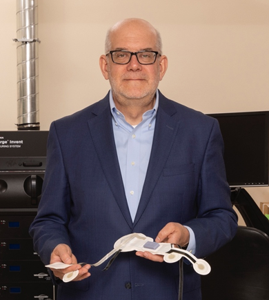 |
Speaker 1: Mark Poliks, Distinguished Professor of Materials Science and Engineering and Systems Science and Industrial Engineering at the Thomas J. Watson College of Engineering and Applied Science, Binghamton University Title: Printing, Placing and Interconnecting Electronic Functions On Available Surfaces: Enabling Hybrid and Additive Approaches To Medical and Industrial Devices |
| 09:45 – 09:50 | Q&A / Transition (5 minutes) | |
| 09:50 – 10:35 |  |
Speaker 2: John H Lau, IEEE Fellow, IMAPS Fellow, ASME Fellow, Senior Packaging Engineer at Unimicron Title: Flip Chip Technology – Solder Bumps, Microbumps, and Bumpless Cu-Cu Hybrid Bonding |
| 10:40 – 11:00 | Break / Networking Session | |
| 11:00 – 11:45 | |
Speaker 3: Rajiv V. Joshi, IEEE Life Fellow, IEEE Daniel Noble Award Winner, Vice President of Industry for IEEE Circuits and Systems Society, Research Scientist at IBM T. J. Watson Research Center Title: Invaluable Memories |
| 11:45 – 11:50 | Q&A / Transition (5 minutes) | |
| 11:50 – 12:35 |
|
Speaker 4: Andreas Kerber, IEEE Senior Member, IEEE Electron Devices Society Distinguished Lecturer, CMOS Reliability Expert at Intel
|
| 12:40 – 13:30 | Lunch |