Static Timing Analysis (STA) Workshop
The IEEE VLSI Student Branch (IEEE VLSI SB) is proud to have successfully organized a two-day hands-on workshop on Static Timing Analysis (STA) on the 27th and 28th of February 2025. This workshop aimed to provide participants with an in-depth understanding of STA concepts and their practical implementation in VLSI design. The session was conducted by Mr. Navneetha Krishnan, a Senior Application Engineer from Entepule Technologies, who shared his extensive knowledge and experience in the field.
Day 1: Inauguration and Introduction to STA Tools
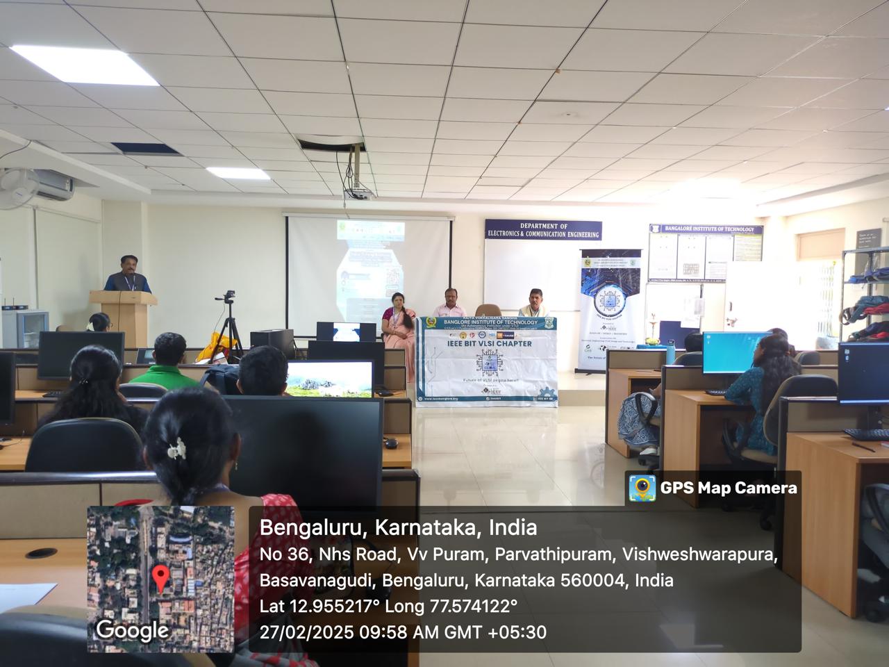
The workshop began with an inaugural session, marking the commencement of an insightful and technical journey into STA. Mr. Navneetha Krishnan introduced the fundamentals of STA and its significance in VLSI circuit design. Participants were given an overview of the Cadence suite of tools used for STA, including Tempus and Innovus. A live demonstration of these tools helped attendees familiarize themselves with the workflow and their functionalities.
One of the key hands-on activities of the first day was scripting an SDC (Synopsys Design Constraints) file. This exercise provided students with a fundamental understanding of how design constraints impact timing analysis and overall circuit performance. The session began with an explanation of various SDC commands and their role in defining timing constraints. Participants learned to specify clock definitions, input and output delays, false paths, and multi-cycle paths using SDC syntax.
To reinforce their understanding, students engaged in practical scripting exercises where they defined constraints for a sample design. The session also included an introduction to scripting techniques using TCL (Tool Command Language), which is widely used in EDA tool automation. Students explored how TCL scripting enhances efficiency by automating repetitive design constraints and modifications.
Additionally, the session emphasized best practices for writing SDC files, ensuring compatibility with tools like Cadence Tempus and Innovus. By the end of the session, participants had successfully created and modified SDC files, gaining hands-on experience in constraint definition. Later, they began working on a counter program, setting the foundation for detailed timing analysis and understanding its implications on setup and hold time constraints.
.
Day 2: Deep Dive into STA Concepts and Practical Analysis
The second day of the workshop commenced with a comprehensive presentation on the theoretical basics of STA. Topics such as slack, skew, rise time, fall time, critical path analysis, setup and hold time violations, and clock timing analysis were thoroughly explained. This session provided participants with the fundamental understanding necessary for effective STA implementation.
Following the presentation, participants engaged in a hands-on session focused on solving STA problems. They analyzed the critical paths of the counter program, identified timing violations, and worked on resolving setup and hold time violations. Clock timing analysis was also performed, allowing students to gain deeper insights into optimizing design performance. The session was highly interactive, with real-time problem-solving and discussions on various STA challenges encountered in industry applications.
The workshop concluded with an interactive Q&A session, where students had the opportunity to clarify doubts and discuss advanced topics related to STA. The knowledge imparted over the two days provided participants with a strong foundation in STA, equipping them with skills highly relevant to the VLSI industry.
To recognize the efforts and participation of attendees, certificates were distributed at the end of the event. IEEE VLSI SB extends its heartfelt gratitude to Mr. Navneetha Krishnan for his expert guidance and valuable insights. The event was a resounding success, providing students with the necessary technical proficiency and hands-on experience in STA, preparing them for future challenges in VLSI design and development.
This workshop proved to be immensely beneficial to students, helping them bridge the gap between theoretical knowledge and industry practices. The practical exposure to Cadence tools, coupled with a deep understanding of STA concepts, has strengthened their technical foundation and enhanced their employability in the semiconductor industry. The skills acquired during this workshop will play a crucial role in their careers, enabling them to tackle real-world challenges in VLSI design with confidence and proficiency.


Date and Time
Location
Hosts
Registration
-
 Add Event to Calendar
- Bangalore Institute Of Technology, Department Of Electronics And Communication, Kr Road, Vv Pura
- Bangalore, Karnataka
- India 560004
- Starts 01 February 2025 06:28 PM UTC
- Ends 25 February 2025 06:32 PM UTC
- No Admission Charge