Distinguished Lecture: Alvin Loke – "The Road to Gate-All-Around and Its Impact on Analog Design"
Despite the much debated end of Moore's Law, CMOS scaling still maintains economic relevance with 3nm finFET SoCs already in the marketplace for over a year and 2nm gate-all-around SoCs anticipated this year. Modest feature size reduction and design/technology innovations co-optimized for primarily logic scaling continue to offer compelling node-to-node power, performance, area, and cost benefits. In this tutorial, we will start with a walk through memory lane, recounting a brief history of transistor evolution to motivate the migration from the planar MOSFET to the fully depleted FinFET. We will summarize the key process technology elements that have enabled the finFET CMOS nodes, highlighting the resulting device technology characteristics and challenges. This will set the context for motivating the introduction of the gate-all-around transistor architecture, namely nanoribbons or nanosheets, and unveiling the magic of how these devices are fabricated. We will then shift to summarize the challenges that CMOS technology scaling has imposed on analog design. To address the growing effort required for analog/mixed-signal design closure, we will cover design strategies on how analog design has adapted and thrived throughout decades of increasingly unfriendly CMOS scaling, including the migration to heterogeneous integration as prophesied by Gordon Moore's seminal 1965 paper.
Date and Time
Location
Hosts
Registration
-
 Add Event to Calendar
Loading virtual attendance info...
- Schatzbogen 7
- Munich, Bayern
- Germany 81829
- Building: NXP Semiconductors Germany GmbH
- Click here for Map
- Contact Event Host
- Co-sponsored by NXP Semiconductors
Speakers
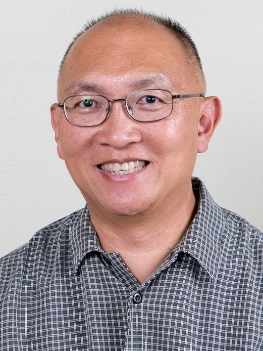
Alvin Loke
Biography:
Alvin Loke is a Senior Principal Engineer at Intel, San Diego, working on analog design/technology co-optimization for Intel’s Angstrom-era CMOS. He has previously worked on CMOS nodes spanning 250nm to 2nm at Agilent, AMD, Qualcomm, TSMC, and NXP. He received a B.A.Sc. in engineering physics from the University of British Columbia, and M.S. and Ph.D. in electrical engineering from Stanford. After several years in CMOS process integration, Alvin has since worked on analog/mixed-signal design focusing on a variety of wireline links, design/model/technology interface, and analog design methodologies. Alvin has been an active IEEE Solid-State Circuits Society (SSCS) volunteer since 2003, having served as Distinguished Lecturer, AdCom Member, CICC Committee Member, Webinar Chair, Denver and San Diego Chapter Chair, as well as JSSC, SSCL, and Solid-State Circuits Magazine Guest Editor. He currently serves as the VLSI Symposium Secretary, SSCS Global Chapters Chair, and again as Distinguished Lecturer. Alvin has authored over 70 publications including the CICC 2018 Best Paper and invited short courses at ISSCC, VLSI Symposium, CICC, and BCICTS. He holds 29 US patents and recently received the ISSCC 2024 Outstanding Forum Speaker Award.


