Digital Lithography: Addressing Scaling Challenges in Advanced Packaging
-- high-performance computing, AI workloads, density, packaging, fine lines, warpage, challenges ...
Requirements on the high-performance compute (HPC) systems from AI workloads necessitates transition to larger package sizes with 2.5D to 3.5D integration and density scaling at every level in the stack. Several competing packaging architectures are emerging to solve the compute and power efficiency challenge presented by AI workloads. Each presents unique lithography challenges such as >100×100 field size, large chip placement deviations, fine lines and tight overlay warped substrates. The conventional lithography tools are incapable of meeting all the requirements to achieve scaling.
The talk will preview Applied Materials’ Digital Lithography Technology (DLT) which enables highest resolution at production throughputs while ensuring CD uniformity and overlay accuracy across the entire panel.
Date and Time
Location
Hosts
Registration
-
 Add Event to Calendar
Loading virtual attendance info...
Speakers
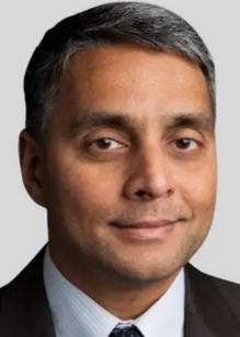
Niranjan Khasgiwale
Biography:
Niranjan Khasgiwale heads marketing for the Digital Lithography BU at Applied Materials.
Niranjan has more than 25 years of experience in the semiconductor equipment industry and joined Applied Materials in 2011 following the acquisition of Varian Semiconductor, where he led strategy and marketing for the implant business unit. He previously held roles with KLA-Tencor and Formfactor.
He holds a Master’s and Ph.D. in Materials Science from Dartmouth College and Lehigh University, respectively, and a B. Tech in Metallurgy from the Indian

Institute of Technology.
Address:Santa Clara, California, United States


