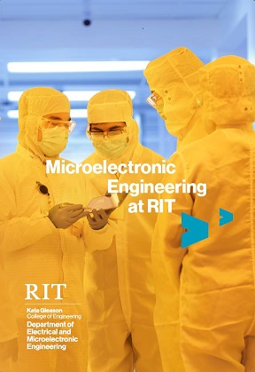
44th Annual Microelectronic Engineering Conference at RIT
Click Here to Register Now! Full Conference Agenda Below!
This conference brings together students, faculty, alumni, friends and industry guests interested in Microelectronic Engineering. Key elements of the conference are: technical presentations by seniors on their capstone research and design projects, industry and alumni presentations, recognition of companies who have supported the program, review of program activities and achievements over the past year and industry feedback on student and academic program activities.
The event begins at 2PM on Monday, 3/13 at the RIT Inn & Conference Center with an industrial program review; all company representatives are welcome and encouraged to attend. The seniors will be showcasing their research projects at the poster session reception at 4PM, followed by a dinner program at 5:30PM. All conference speakers, faculty, Microelectronic Engineering seniors and graduate students, and members from industry are invited.
Off-campus map - RIT Inn & Conference Center
The technical session is on Tuesday, 3/14 from 8AM - 4:30PM in the Center for Integrated Manufacturing (CIMS, SLA/078). Student talks and invited speakers are in morning and afternoon sessions, divided by a noon lunch catered by Dinosaur BBQ!
Campus map - CIMS Conference Center
Registration is required (no charge) to determine meal orders.
Date and Time
Location
Hosts
Registration
-
 Add Event to Calendar
- Rochester Institute of Technology
- One Lomb Memorial Drive
- Rochester, New York
- United States 14623
- Building: CIMS / Slaughter Hall SLA/078 (campus map)
- Room Number: 2210 - 2240
- Click here for Map
- Contact Event Host
-
Karl Hirschman (click above)
Michael Jackson, majemc@rit.edu (email)
- Starts 20 March 2026 04:00 AM UTC
- Ends 15 April 2026 03:59 AM UTC
- No Admission Charge
Speakers
Bryan Kasprowicz of HOYA Corporation
System Level Co Optimization of Absorber and Multilayer Stacks for Next Generation EUV Mask Blanks
EUV mask blank technology continues to advance rapidly as the semiconductor industry pushes toward higher‑NA lithography, improved productivity, and smaller patterning nodes. This work integrates recent developments in absorber materials, multilayer design, and durability evaluation. Defect minimization remains the primary requirement, with current EUV blanks achieving zero phase defects suitable for 3 nm applications. While Ta‑based binary absorbers have enabled early high‑volume EUV manufacturing, low‑n attenuated phase‑shifting absorbers demonstrate enhanced NILS and potential throughput gains. Parallel efforts on alternative multilayers show reduced effective mirror plane depth, improving non‑telecentricity, though with inherent reflectivity trade‑offs. Compensation methods using optimized absorbers and mask bias are explored. Durability testing with hydrogen‑plasma exposure confirms strong correlation to scanner environments and no multilayer damage. Additionally, tri‑tone and multilayer‑etch black‑border structures are evaluated to mitigate EUV and out‑of‑band light for future high‑NA systems. These results underscore the need for holistic co‑optimization of absorber, cap, and multilayer stacks to meet next‑generation EUV requirements.
Biography:
Bryan S. Kasprowicz, BS MicroE 1996
Sr. Director, Technical Strategy at HOYA Corporation, USA

Biography: Bryan S. Kasprowicz is a seasoned technology executive and recognized expert in photomask technology, semiconductor lithography, and advanced manufacturing processes for the electronics industry.
With three decades of experience, Mr. Kasprowicz has held senior leadership roles at leading companies in the photomask and materials sector, including serving as Senior Director of Technical Strategy at HOYA Corporation (HOYA Electronics/IT segment), where he drives technical innovation and strategic direction for next-generation photomask solutions. His earlier career included significant contributions at Photronics, Inc., where he advanced research and development in mask materials, etching processes, phase-shift masks (PSM), optical proximity correction (OPC), and extreme ultraviolet (EUV) lithography technologies and Texas Instruments Inc., focused on advanced lithography processes, including the insertion of copper using dual damascene.
A prolific contributor to the field, Mr. Kasprowicz has authored or co-authored over 40 technical publications, including three Best Paper Awards, and holds multiple patents related to photomask design, materials evaluation, and patterning techniques critical to enabling smaller nodes in semiconductor fabrication (including work on 65nm and beyond). He has presented at major industry conferences such as SPIE Photomask Technology, Photomask Japan, and others, often addressing challenges in EUV photomasks, multiple patterning, and mask topography effects.
Mr. Kasprowicz is a long-standing Senior Member of SPIE (the international society for optics and photonics), with over 29 years of membership. He has been honored as an SPIE Community Champion (2019 and 2020) for his dedication to advancing the field through education, collaboration, and leadership. He also serves as a panelist on topics ranging from next-generation mask materials to unsolved issues in advanced photomasks. He received a Bachelor of Science degree in microelectronics engineering from Rochester Institute of Technology in 1996 and maintains active involvement in shaping the future of semiconductor patterning technologies that power the global electronics ecosystem.
Patrick Naulleau of EUV Tech Inc.
Critical Actinic Mask Metrologies in the EUV Regime
Extreme ultraviolet lithography has enabled the semiconductor industry to continue on the long-term path of patterning shrink. Impressively, the industry is now approaching the atomic scale, where the quantized nature of light and materials is becoming a very significant limiter to the ultimate performance of the patterning process. While stochastics on the photoresist side has justifiably attracted much attention over the past few years, stochastic processes also have important implications on EUV mask characteristics which in turn ripple down to observed patterning stochastics including effects such as line-width roughness and contact hole critical dimension uniformity problems. It will be shown that, fundamentally, these problems arise from phase stochastics on the mask and that only actinic metrology is directly sensitive to these effects. In the second half of the presentation, focus will be turned to applying these same actinic scattering metrologies to the characterization of indented EUV phase shift structures instead of the undesired stochastic phase noise discussed above. In this section, the sensitivity of the EUV phase shift mask to various critical parameters such as wavelength, illumination angle, and pitch is explored. These effects are used to highlight some of the challenges and constraints in the application of phase shift masks in the EUV regime.
Biography:
Patrick Naulleau
CEO, EUV Tech Inc.
San Francisco Bay Area

Biography: Patrick Naulleau received his B.S. and M.S. degrees in electrical engineering from the Rochester Institute of Technology, Rochester, NY, in 1991 and 1993, respectively. He received his Ph.D. in electrical engineering from the University of Michigan, Ann Arbor in 1997 specializing in optical signal processing and coherence theory. In 1997 Dr. Naulleau joined Berkeley Lab on the EUV LLC program building the world’s first EUV scanner. From June 2005 through March 2008, Dr. Naulleau additionally joined the faculty at the University at Albany, SUNY as Associate Professor, also concentrating in the area of EUV lithography. In April 2010 Dr. Naulleau took the position of Director of the Center for X-ray Optic at Lawrence Berkeley National Laboratory establishing and running their world-leading EUV high-NA lithography/metrology research facility through 2022. In August 2022, Dr. Naulleau assumed the role of CEO at EUV Tech Inc., a leading supplier of EUV metrology equipment. Dr. Naulleau has over 400 publications as well as 20 Patents and is a Fellow of SPIE and Optica.
Robert Mulfinger of GlobalFoundries
GlobalFoundries Next Gen Photonics Device Offering: Enabling the Future of AI
Exponential growth of Artificial Intelligence (AI) and Large Language Models (LLMs) is imposing unprecedented demands on data centers, leading to significant challenges in data transport, bandwidth, and power consumption that conventional electrical interconnects struggle to meet. Optical interconnect technologies, powered by silicon photonics, are emerging as a critical solution to these bottlenecks, enabling data transmission at the speed of light with significantly higher bandwidth, lower latency, and greater energy efficiency compared to traditional copper-based systems.
GlobalFoundries (GF) is at the forefront of this technological shift, leveraging its leading silicon photonics (SiPh) foundry capabilities to enable the future of AI. More specifically, GF's Next Gen photonics offering is positioned to fully unlock optical interconnects by leveraging recent advancements in device bandwidth, advanced data transport, and optimized integrations to enable fiber attach, on die lasers and advanced test.
Biography:
Bob Mulfinger
uE/Material Science BS/MS ‘06
Senior Manager/Dep. Dir Device Engineering
GlobalFoundries (GF)

Biography: Bob Mulfinger received B.S. degree in Microelectronic Engineering and a M.S. degree in Materials Science from the Rochester Institute of Technology in 2006. Since then, he has worked for AMD/GF as a product engineer, integration engineer and device engineer spanning technologies from 90nm down to 7nm including planar PDSOI, FINFET, FDSOI and silicon photonics. Bob is a GlobalFoundries Master Inventor and holds over 40 patents. He is currently leading the silicon photonics device, test and characterization teams in Malta, NY.
Melinda Murdock of Intel Corporation
Designing Talent, Manufacturing the Future
As the semiconductor industry expands to meet growing global demand, workforce development has become a critical priority for industry and national competitiveness. In this talk, Mindy Murdock shares insights from her 30+ year career at Intel, culminating in her current role supporting workforce development through university research and collaborations. The presentation will include a brief overview of Intel as an Integrated Device Manufacturer (IDM), where both design and manufacturing play essential and interconnected roles in delivering advanced semiconductor technologies. Mindy will discuss how this dual focus drives unique workforce needs across engineering, manufacturing, and technical disciplines. Drawing on her experience, she will highlight current efforts to build a strong semiconductor talent pipeline through partnerships with academia, curriculum development, and inclusive pathways into the industry. The talk will also explore why investing in a skilled semiconductor workforce is vital to innovation, economic growth, and national security.
Biography:
Melinda Murdock
University Program Director, Intel
Chandler, Arizona

Biography: Melinda (Mindy) Murdock has over 30 years of experience at the Intel Corporation, where she has held a range of roles across engineering, ecosystem development, and university engagement. She currently serves as a Program Director for the University Research & Collaborations group within the Intel Labs, focusing on aligning academic partnerships with Intel’s long-term semiconductor and advanced technology needs. Throughout her career, Mindy has worked closely with industry partners, universities, and government organizations to align technology roadmaps, strengthen research collaboration, and build talent pipelines. Her work today centers on workforce development and helping ensure a strong, future-ready semiconductor workforce. Mindy holds a Bachelor of Science in Computer Science from Rochester Institute of Technology and an Associate’s degree from Tompkins Cortland Community College.
Agenda
Evening Program
6:30 pm Welcome, Invited Speaker, Awards
Invited Talk: “Designing Talent, Manufacturing the Future” by Mindy Murdock, University Program Director, INTEL
8:00 pm Closing Remarks
8:00 – 8:30 a.m. Registration
Morning Session AM-1
Session Chair: Dr. Robert Pearson, Professor Emeritus in MicroE, RIT
8:30 a.m. Welcome: Karl Hirschman, Microelectronic Engineering Program Director
8:35 a.m. Opening Remarks: Ferat Sahin, Department Head Electrical and Microelectronic Engineering, RIT
8:40 a.m. Invited Talk: “Holistic Look at the Development of Next Generation EUV Mask Blanks”, Bryan Kasprowicz, Sr. Director, Technical Strategy at HOYA Corporation, IT Segment Company
9:10 a.m. “Fabrication of Vertical GaN FinFETs”, Jason Lonneville, BS MicroE ‘26
9:25 a.m. “Measuring Dynamic Conduction and Coss Losses in GaN FETs”, Noah Donner, BS MicroE ‘26
9:40 a.m. “Etch Investigation of Materials and Selectivity to Support Double Patterning Workflow”, Jade Devilliers, BS MicroE ‘26
9:55 a.m. “Self-Alignment Using Monolayer Doping”, Farhaanuddin Mohammed, BS MicroE ‘26
10:10 a.m. BREAK
Morning Session AM-2
Session Chair: Dr. Karl Hirschman, Micron Professor in MicroE, RIT
10:30 a.m. Invited Talk: “Critical Actinic Mask Metrologies in the EUV Regime”, Patrick Naulleau, CEO, EUV Tech, Inc.
11:00 a.m. “Optimization of Growth and Fabrication Conditions to Realize an InP/InGaAs HBT”, Mason Wolcott, BS MicroE ‘26
11:15 a.m. “Characterization of LPCVD Polysilicon”, Ben Infante, BS MicroE ‘26
11:30 a.m. “Investigations of Single-Crystal Silicon-on-Glass (SiOG) Substrate for Next Gen Display Devices”, Matt Lynch, BS MicroE ‘26
11:45 a.m. “Encouraging Young Minds Toward Microelectronic Engineering”, Elissa Sainthil, BS MicroE ‘26
12:00 p.m. LUNCH – Dinosaur BBQ
Afternoon Session PM-1
Session Chair: Sean Rommel, Professor in MicroE, RIT
1:00 p.m. Invited Talk: “GlobalFoundries Next Gen Photonics Device Offering: Enabling the Future of AI”, Bob Mulfinger, Sr. Manager, Dep. Dir. Device Engineering, GlobalFoundries (GF)
1:30 p.m. “Fabrication of InP Micropillar Arrays via ICP-RIE: A Parameter Space Exploration”, Aiden Prunoske, BS MicroE ‘26
1:45 p.m. “Influence of Spin-On Doping of Si MacEtch towards Applications in Photovoltaics”, Race Printup, BS MicroE ‘26
2:00 p.m. “16-Bit D-2D Digital to Analog Converter Design”, Toby Mogendorff, BS MicroE ‘26
2:15 p.m. “Comparing Off-Axis and Conventional Exposure Techniques’, Scott Gerber, BS MicroE ‘26
2:30 p.m. BREAK
Afternoon Session PM-2
Session Chair: Santosh Kurinec, Professor in MicroE, RIT
2:50 p.m. “Cascade Probe Station and Keithley 4200 Parameter Analyzer Testing Development”, Aiden Maraia, BS MicroE ‘26
3:05 p.m. “Gate Oxide Integrity”, Yousuf Karim, BS MicroE ‘26
3:20 p.m. “RIE vs. IBE: Process Replacement Study”, Stephanie Ye, BS MicroE ‘26
3:35 p.m. “Defect Density and Yield Estimation for Critical CMOS Layers”, Louis Fleischer, BS MicroE ‘26
3:50 p.m. “Process Integration and Fabrication of Torsion Bar-Based Micromirrors”, Brandon Rinaldi, BS MicroE ‘26
4:05 p.m. Concluding Comments
4:15 p.m. Adjourn