

Technical Talk on “Electronic Semiconductor Devices, From Fundamentals to Innovation”


The IEEE CEDA DSCE Student Chapter organized a Technical Talk on “Electronic Semiconductor Devices, From Fundamentals to Innovation” on 9th May 2026 at the Department of Electronics and Communication Engineering, Dayananda Sagar College of Engineering (DSCE), Bengaluru. The objective of the workshop was to provide students with practical exposure and conceptual understanding of semiconductor devices, their evolution, and recent innovations in semiconductor technology.
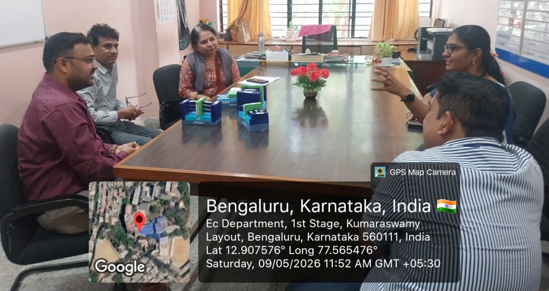
The session was delivered by Mr. Utkarsh Garg, Senior Staff Engineer at Samsung Semiconductor India R&D, who possesses extensive industry experience in semiconductor device technologies and VLSI design. The workshop began with a warm welcome to the speaker, faculty members, IEEE members, and student participants. The resource person was formally introduced, highlighting his expertise and contributions to the semiconductor industry. As a gesture of gratitude and appreciation, the organizing team honored the speaker with a sapling. This symbolic gesture reflected the institution’s respect and appreciation for the speaker’s valuable contribution towards student learning and professional development.
During the workshop, the speaker explained the evolution of semiconductor devices starting from vacuum tubes and BJTs to modern MOSFET technologies. He discussed the significance of MOSFETs in modern electronics and elaborated on important concepts such as Moore’s Law, Dennard Scaling, and Koomey’s Law. The session further explored advanced semiconductor technologies including FinFETs, MBCFETs, Forksheet transistors, and CFET technologies.The speaker also highlighted the importance of technology scaling, energy efficiency, and advanced transistor architectures in modern semiconductor industries. Concepts related to standard cell libraries, ASIC design methodologies, and the growing role of Artificial Intelligence in semiconductor design automation were discussed in detail.
The workshop was highly interactive, with students actively participating in discussions and clarifying their doubts regarding semiconductor technologies, VLSI design, and industry opportunities. The session successfully bridged theoretical concepts with real-world semiconductor applications and provided students with valuable industry-oriented insights.
Overall, the event was informative, interactive, and successful in motivating students to explore advanced semiconductor technologies and career opportunities in VLSI and chip design.
 |
 |
 |
 |
 |
Date and Time
Location
Hosts
Registration
-
 Add Event to Calendar


- #101, Seminar Hall, Building No.01
- Heritage Block Dayananda Sagar College of Engineering
- Bengaluru, Karnataka
- India 560078
Speakers
Utkarsh Garg of Samsung Semiconductor India R&D